Layout Design Rules
The layout design rules provide a set of guidelines for constructing the various masks needed in the fabrication of integrated circuits. Design rules are consisting of the minimum width and minimum spacing requirements between objects on the different layers.
The most important parameter used in design rules is the minimum line width. This parameter indicates the mask dimensions of the semiconductor material layers. Layout design rules are used to translate a circuit concept into an actual geometry in silicon.
The design rules is the media between circuit engineer and the IC fabrication engineer. The Circuit designers requires smaller designs with high performance and high circuit density whereas the IC fabrication engineer requires high yield process.
Minimum line width (MLW) is the minimum MASK dimension that can be safely transferred to the semiconductor material. For the minimum dimension design rules differ from company to company and from process to process.
To address this issue scalable design rule approach is used. In this approach rules are defined as a function of single parameter called 'l'. For an IC process 'l' is set to a value and the design dimensions are converted in the form of numbers. Typically a minimum line width of a process is set to 2l e.g. for a 0.25 mm process technology 'l' equals 0.125 mm.
Layered Representation of Layout :
The layer representation of layout converts the masks used in CMOS into a simple layout levels that are easier to visualise by the designers. The CMOS design layouts are based on following components :
(1) Substrates or Wells : These wells are p type for NMOS devices and n type for PMOS devices.
(2) Diffusion regions : At these regions the transistors are formed and also called as active layer. These are defined by n+ for NMOS and p+ for PMOS transistors.
(3) Polysilicon layers : These are used to form the gate electrodes of the transistors.
(4) Metal interconnects layers : These are used to form the power supply and ground rails as well as input and output rails.
(5) Contact and Via layers : These are used to form the inter layer connections.
CMOS-Layout-Design
![]() Layout of Logic gates:
Layout of Logic gates:
![]() Three Input NAND Gate :
Three Input NAND Gate :
Figure below shows, the schematic, stick diagram and layout of three input NAND gate.

Two Input NAND Gate :
Figure below shows the schematic, stick diagram and layout of two input NAND gate implemented using complementary CMOS logic.

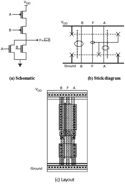
Two Input NOR Gate :
Figure below shows the schematic, stick diagram and layout of two input NOR gate implemented using complementary CMOS logic.

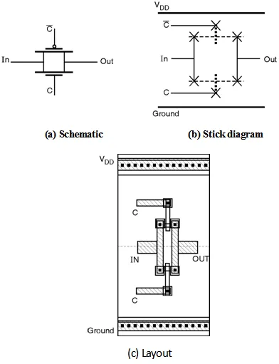
Transmission Gate :
Figure below shows the schematic, stick diagram and layout of the transmission gate.
