Pass Transistor
The Low-Resistance Path
The basic answer to this question is that logic high indicates a voltage at the supply rail, representing a binary 1, and logic low indicates a voltage at ground, representing a binary 0. This description is a good place to start, and it becomes more accurate if we say “near the supply rail” and “near ground” instead of “at the supply rail” and “at ground.” This modification accounts for the fact that currents flowing through the channel of the NMOS or PMOS create a small voltage difference between source and drain.
This issue of current flow through the channel leads to a more subtle, but nonetheless crucial, aspect of typical CMOS functionality. A CMOS inverter ensures that the output node will have a low-resistance connection to the supply rail or ground; the inverter always has the NMOS conducting and the PMOS in cutoff or the PMOS conducting and the NMOS in cutoff. This is why we can say that CMOS circuits drive a logic low or logic high. It is also why logic circuits built around the inverter topology are so reliably “digital”—all the nodes have a clearly defined binary state because they always have a low-resistance path to the supply voltage or ground.
Pass-transistor logic (PTL), also known as transmission-gate logic, is based on the use of MOSFETs as switches rather than as inverters. The result is (in some cases) conceptual simplification, but the CMOS inverter’s strict logic-high/logic-low output characteristic is lost.
An Example of Pass-Transistor Logic
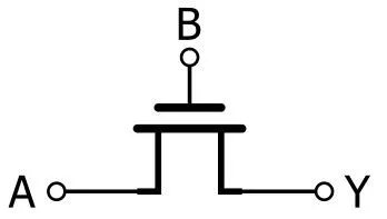
It is possible to use a single NMOS transistor as a PTL switch; the switch is considered closed when the voltage applied to the gate is logic high, and it is considered open when the voltage applied to the gate is logic low. The following diagram shows an AND gate (or at least something similar to an AND gate) that uses only one transistor.
Note that I’ll be using the “circle vs. non-circle” MOSFET symbols; see this article for more information.
The output (Y) is logic high when the input (A) is logic high and the switch-control signal (B) is logic high, and it is not logic high for all other combinations. That sounds like the AND truth table, but can we really call this an AND gate? That depends on your perspective. The problem is that the circuit doesn’t drive a logic low when the B input is logic low. It’s simply disconnected, i.e., floating. To establish a logic low, we need a pull-down resistor:
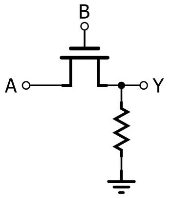
Now we have a functional AND gate, and we’ve used only one transistor and one resistor, whereas a standard CMOS-inverter-based AND gate requires six transistors. However, the PTL circuit is by no means equivalent to the standard CMOS version. First of all, it does not reliably provide a low-resistance path to ground. Second, it dissipates static power whenever the output is logic high—current flows from the input, through the NMOS, through the pull-down resistor, to ground:
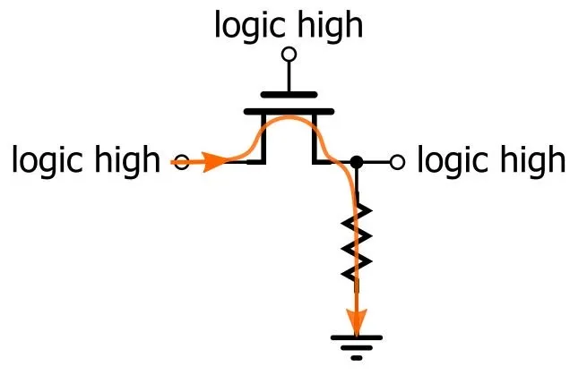
This means that we have lost an extremely beneficial property of inverter-based logic, namely, that the power supply delivers significant amounts of current only during switching. (That’s why CMOS power dissipation is proportional to frequency—more switching means more current, and more current means more power.)
NMOS vs. CMOS in Pass-Transistor Logic
As demonstrated in the preceding section, PTL is built around MOSFET switches that either pass (hence the name) or block a signal. Using an NMOS transistor as the switch is certainly a good way to reduce transistor count, but a lone NMOS isn’t impressive in terms of performance. A much better solution is the CMOS transmission gate:
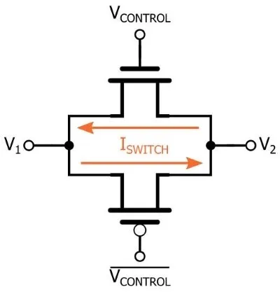
The lone NMOS and the CMOS transmission gate are briefly compared in this article. There’s no doubt that the transmission gate is, in general, the superior implementation, but consider the trade-off. Obviously an additional transistor is required, but note also that the PMOS is driven not by the switch-control signal but by the complement of the switch-control signal. This is not a problem if the circuit that generates the input signal is, for example, a D flip-flop that provides both a [Math Processing Error]Q and a [Math Processing Error]Q¯ output. Usually, though, only one input signal is available, and in such cases the use of a CMOS transmission gate means that we must also have an inverter to create the control signal for the second FET.
Assessing Pass-Transistor Logic
At this point you may be wondering why I bothered to write an article about such a decidedly mediocre version of MOSFET-based digital logic. The overwhelming dominance of standard CMOS circuitry is enough to confirm that PTL has limited usefulness.
However, it’s critical to understand that carefully designed PTL implementations can provide acceptable functionality while reducing transistor count. Even if the reduction is small relative to an individual subcircuit, such as an XOR gate or a flip-flop, the overall effect can be significant in a device that includes thousands of identical subcircuits. In a follow-up article I’ll present advantageous PTL versions of widely used digital circuits.