Microwave Transistors
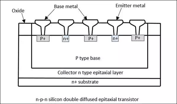
There is a need to develop special transistors to tolerate the microwave frequencies. Hence for microwave applications, silicon n-p-n transistorsthat can provide adequate powers at microwave frequencies have been developed. They are with typically 5 watts at a frequency of 3GHz with a gain of 5dB. A cross-sectional view of such a transistor is shown in the following figure.

Construction of Microwave Transistors
An n type epitaxial layer is grown on n+ substrate that constitutes the collector. On this n region, a SiO2 layer is grown thermally. A p-base and heavily doped n-emitters are diffused into the base. Openings are made in Oxide for Ohmic contacts. Connections are made in parallel.
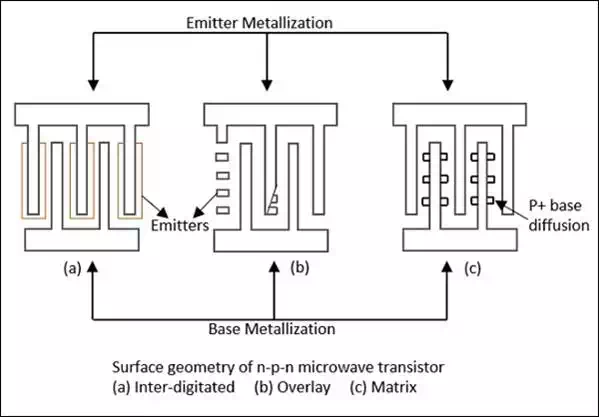
Such transistors have a surface geometry categorized as either interdigitated, overlay, or matrix. These forms are shown in the following figure.

Power transistors employ all the three surface geometries.
Small signal transistors employ interdigitated surface geometry. Interdigitated structure is suitable for small signal applications in the L, S, and C bands.
The matrix geometry is sometimes called mesh or emitter grid. Overlay and Matrix structures are useful as power devices in the UHF and VHF regions.
Operation of Microwave Transistors
In a microwave transistor, initially the emitter-base and collector-base junctions are reverse biased. On the application of a microwave signal, the emitter-base junction becomes forward biased. If a p-n-p transistor is considered, the application of positive peak of signal, forward biases the emitter-base junction, making the holes to drift to the thin negative base. The holes further accelerate to the negative terminal of the bias voltage between the collector and the base terminals. A load connected at the collector, receives a current pulse.