New Chip Technology Shows Off the Next Big Step in Moore’s Law
Increasingly, modern life depends on how skillfully we shuttle electrons through the nanoscale mazes etched on computer chips. These processors aren’t just for laptops anymore—they’re used in your car, your thermostat, your refrigerator and microwave.
And the pandemic has revealed just how deeply our dependence runs.
A global shortage of computer chips, brought on by vacillating demand and supply chain issues, is currently rippling through device-makers, of course, but also makers of cars, vacuum cleaners, and stove vents.
Clearly, we’re hooked.
So, perhaps it’s no surprise that when companies announce better, faster, more efficient computer chips, the world takes notice. This week, it was IBM’s turn to make headlines.
The company, once synonymous with all things computing, announced that it’s demonstrated a 2-nanometer (nm) chipmaking process for the first time.
In a press release, IBM said the new process would yield some 50 billion transistors on a chip the size of a fingernail. It would also bring chips that are 75 percent more efficient or 45 percent faster than today’s 7-nm chips.
On its face, it would seem IBM just leapt far ahead in the race for top chip tech. Intel’s latest chips use a 10-nm process and TSMC’s use a 7-nm process. And the company has made some very cool and notable progress here. But comparing chips is complicated. So, it’s worth dissecting the news a bit more to better understand the bigger picture.
Nanometer to Nanometer Is Apples to Oranges
Progress in computer chips has long been measured in nanometer-sized steps. Each step down yields ever more components—most notably, transistors—packed into the same area. And there was a time, in decades past, when the nanometer nomenclature actually did match the size of certain chip elements. But that time has passed. As chip technology advanced, the measurements of chip components decoupled from each generation’s naming convention.
By the time chips made the last big leap to FinFET—a 3D transistor design shaped like a fin—a little over a decade ago, the industry’s node number was virtually meaningless. It didn’t relate to any dimension on the chip. There’s currently a debate over what new number, or combination of numbers, better reflects progress. And although this too is proving rather complicated, one spec experts propose is transistor density per square millimeter.
To see how the old naming convention is confusing, compare Intel’s 10-nm chips with TSMC’s 7-nm chips. The two actually have roughly equivalent transistor densities, with Intel’s 100 million transistors per square millimeter actually edging out TSMC’s 91 million per square millimeter. (Go here for a handy table comparing process size and transistor density of chips.)
IBM didn’t announce transistor density explicitly. But after reaching out to clarify exactly what sized “fingernail” they were referencing—representatives of the company said about 150 square millimeters—the publication AnandTech calculated IBM’s new process would yield some 333 million transistors per square millimeter. Which is, indeed, beyond anything in production. That said, a 3-nm chip TSMC is making for Apple could boast almost 300 million transistors per square millimeter and enter production as soon as next year.
Nanosheets: The Next Step in Moore’s Law?
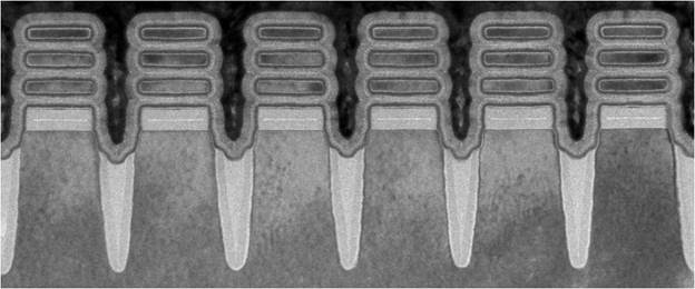
Perhaps the more significant news is the design of the transistors themselves. IBM’s new technology—called nanosheet or gate-all-around transistors—is the long-awaited successor to today’s FinFET transistors. The company has been working on the tech since 2017.
FinFET transistors consist of a fin-shaped channel surrounded on three sides by a “gate” that controls the flow of electrons. But IBM’s nanosheet (or gate-all-around) transistors have a layered channel instead. The layers are stacked on top of each other and, like three pigs-in-a-blanket, are surrounded by the gate on all sides. This last bit is the most critical piece. Gate-all-around transistors provide better control of current through the channel, prevent leakage, and boost efficiency.