Photonic Ising machine
Numerous important applications, such as circuit design, route planning, sensing, and drug discovery can be mathematically described by combinatorial optimization problems. Many of such problems are known to be non-deterministic polynomial time (NP)-hard or NP-complete problems. However, it is a fundamental challenge in computer science to tackle these NP problems by conventional (von Neumann) computing architecture since the number of computational states grows exponentially with the problem size. This challenge motivates large amount of research work attempting to develop non von Neumann architectures. Fortunately, Ising model provides a feasible way to efficiently solve these computational-hard problems by searching the ground-state of the Ising Hamiltonian . Various schemes of simulating Ising Hamiltonian have been proposed and experimentally demonstrated in different physical systems, such as superconducting circuits , trapped ions , electromechanical oscillators , CMOS devices , memristors , polaritons and photons ,Among these systems, photonic system has been considered as one of the most promising candidates due to its unique features, such as inherent parallelism, low latency and nearly free of environment noise, namely thermal and electromagnetic noise. In this section, the brief reviews of recent progress of photonic Ising machine (denoted as PIM hereafter) have been given and the main hurdles that hamper its practical applications have been clarified.
Before reporting research progress during last decade, the concept of Ising model is explained as follow. Figure 5(a) explicitly illustrates an Ising model with N = 5 spin nodes. Each node occupies one spin state, either spin-up (σi = + 1) or spin-down (σi = − 1). Ji, j represents interaction between two connected spins σi and σj. The Hamiltonian of Ising model without external field is given by
H=-∑1≤i<j≤NJi,jσiσj.H=-∑1≤i<j≤NJi,jσiσj.
(5)
Fig. 5
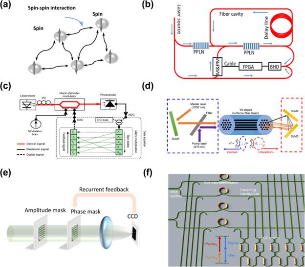
Overview of optical Ising machine. a Ising model. b Schematic of coherent Ising Machine (CIM) based on degenerate OPO. c Ising machine works in nonlinear regime of modulator . d Ising machine based on multi-fiber. e Simulated annealing based on SLM. f Schematic of all-optical Ising machine [151]. Figures adapted under a CC BY 4.0 licence from ref. (c), ref. (d), ref. (f)
Driven by the interaction network and the underlying annealing mechanism, the Ising model could gradually converges into a particular spin configuration that minimizes the energy function (H). Three annealing mechanisms are illustrated in Fig. 5(b). One mechanism is simulated annealing (denoted as SA hereafter) relies on a specific annealing algorithm. Other two annealing mechanisms belong to a broad class of physical annealing (denoted as PA hereafter). Specific speaking, one is quantum annealing that harnesses quantum tunneling effect to identify the minimum state. The last one is optical parametric oscillation (OPO) gained network which relies on the mode selection in the dissipative system. Here, apart from the OPO network, there are other peculiar mechanism being used to realize physical annealing as well, such as nonlinear dynamics in opto-electronic oscillators (OEO) .
Figure 5(a) and (b) indicates four indispensable elements of Ising machine: spin node, interaction network, feedback link and annealing mechanism. Taking advantages of various degrees of freedom and appropriate technologies, numerous schemes have been experimentally demonstrated during last decade .Figure 5(c) to (f) show several exceptional works of PIM . Meanwhile, the experimental data of relevant works is summarized in Table 1. Additionally, scalability and robustness are included in our discussion with the consideration of potential practical applications. These experimental demonstrations can be classified into three classes: fiber-based systems, free-space systems and chip-based systems. Each system is briefly explained in the next paragraph.
Fiber-based systems are shown in Fig. 5(b) and (c). Each spin node is represented by an optical pulse and their interaction network is implemented by optical delay or field programmable gate array (FPGA) . One advantage of fiber-based system is the excellent scalability that allows large-scale Ising model by increasing cavity length or repetition rate, while it suffers robustness issue result from a relatively short coherent time of photon. A mitigated approach is encoding the spin state in microwave signal since its coherent time is way longer than an optical signal . Moreover, temporal multiplexing scheme constraints the scope of its applications as sequential processing sacrifices large part of annealing time. Figure 5(d) and (e) illustrate free-space systems. Spin node and interaction network are implemented by a fiber-core (or a pixel) and a SLM, respectively. In spatial domain, free-space system allows large-scale Ising model annealing simultaneously. Nevertheless, inevitable fluctuations in practical environment will ruin the interaction network as it relies on the accurate alignment. Chip-based systems are shown in Fig. 5(f). A fully reconfigurable interaction network is implemented by MZI matrix . And the spin node can be built by a scalable building block, such as micro-ring resonator . Benefiting from the advanced CMOS technologies, chip-based system could potentially shrink a clumsy system into one monolithic/hybrid chip so that it is nearly immune from environmental fluctuation. Compared with the spin node demonstrated in other two classes, chip-based system is the “ugly-duckling” of approach to PIM. It will grow into a swan after we tackle several technical challenges. These challenges will be included into the following discussion.
Based on these extensive research woks, the technical roadmap of PIM becomes crystal clear. It is to develop a highly scalable, reconfigurable and robust PIM that could find an optimal (or a near optimal) solution of a large-scale combinatorial optimization problem in a polynomial time. Table 1 indicates the fiber-based scheme and the chip-based scheme are two promising pathways as they satisfy scalability and robustness simultaneously. However, both schemes are severely limited by the scale of the interaction network since practical applications requires large amount of spin node. In fiber-based scheme, a creative solution is rebuilding the feedback signal after balanced-homodyne detection (BHD) and VMM in FPGA . The cost is extra process time required for synchronization between the optical signals within cavity and the external feedback signals. Besides additional time consumption, electro-optical conversion and VMM in FPGA are the potential bottleneck for the large-scale PIM. One plausible solution is utilizing N − 1 optical delay lines with modulator in each line so that generate feedback signal instantaneously .
In chip-based scheme, the interaction network requires an overwhelming number of optical unit (∝N2, where N represents spin number) . To the best of our knowledge, the largest MZI matrix (64*64) developed by Lightmatter is still smaller than the dimension of practical models . Alternatively, nonlinear effect, such as frequency conversion via χ(2) / χ(3) medium , could be a viable approach to build interaction network on a large scale. Meanwhile, the giant model of practical problems can be split into many sub-models so that we can solve these sub models sequentially or simultaneously by chip-based systems with a comparable matrix size. Besides the aforementioned technical challenges, experimental verification of the parallel search or the ergodicity of spin configuration in PIM, particularly in coherent Ising machine (CIM) , is another haunting research work. Because this work would explicitly explain the advantage of PIM over von Neumann computing architecture.
The promising results of PIM achieved over last decade indicate a feasible way to solve computational hard-problems. However, this research direction needs continuous research effort to build a scalable, reconfigurable and robust PIM which will make profound impact on our society.