Analog optical computing: an alternative approach at post-Moore era
Optical computing is not a brand-new concept. Back to the middle of twentieth century, the optical correlator had already been invented , and it can be treated as an preliminary prototype of optical computing system. Other technologies underpinned by the principles of Fourier optics, such as 4F-system and vector matrix multiplier (VMM), were well developed and investigated during last century . The great success of digital electrical computer promotes the investigations of digital optical computer in which the optical logic gates have been concatenated . The idea of replacing electrical transistor by optical transistor was considered as a competitive approach to build a digital optical computer due to the intrinsic merits of photon, such as high bandwidth, negligible heat generation and ultra-fast response. However, this tantalizing idea has not yet been systematically verified since the middle of twentieth century. D. B. Miller proposed some practical criteria for optical logic in 2010, and he pointed out that current technologies were incompetence to meet these criteria. These criteria include logic-level restoration, cascadability, fan-out, input–output isolation, absence of critical biasing and independent loss at logic level . Until now, a digital optical computer is still a fascinate blueprint. Digital electrical computer still is a practical and reliable system due to its compatibility and flexibility. Alternatively, analog optical computing harnessing physical mechanisms opens up new possibilities for optical computing because it relieves the requirement of high integration density by implementing arithmetic operation rather than Boole logic operation. In this chapter, VMM, reservoir computing and photonic Ising machine are illustrated as three typical instances of analog optical computing. “Vector and matrix manipulation in optical domain” section explains the principle of VMM and its applications toward complex computing. “Optical reservoir computing” section and “Photonic Ising Machine” section summarize the principle and research progresses of reservoir computing and photonic Ising machine, respectively.
Vector and matrix manipulation in optical domain
Since optical computing has not yet been verified as a viable approach to realize universal computing via logical operations, people start to explore the potential opportunities in arithmetic computing, such as multiplication and addition. In this section, the relevant researches are briefly summarized and sequentially explained. Firstly, a principle explanation of multiplication is followed by a typical realization called fan-in/out VMM introduced by Goodman in last century. Many creative schemes and new technologies are introduced as well. Then complex computing is introduced, such as Fourier transformation (FT) and convolution. A typical way of realizing FT and convolution are explicitly explained. At last, other optical computing schemes are mentioned as well.
VMM-vector matrix multiplier
As mentioned above, the first fan-in/out VMM was proposed as early as 1978 . This multiplier is designed to compute multiplication between a vector and a matrix as follows
Cj=∑iBji⋅Ai,Cj=∑iBji⋅Ai,
where A and B are a vector and matrix, respectively. The jth-row of the matrix B times with the vector A in an element-wise way, and a scalar result Cj is obtained after summation. After traversing each row of matrix B, the final result of the VMM is obtained.
The traditional free-space fan-in/out VMM scheme shows in Fig. 1(a). The input vector A and matrix B are loaded into an array of light sources and a series planar spatial light modulators (SLM), respectively. One or several lenses are used to expand each light beam from a Ai source to illuminate all the pixels at i-th column of SLM. Then, a cylinder lens (other collimating lenses may be used to improve the precision) is used to focus all the beams in the horizontal direction, and a line array of spots can be detected at last. Theoretically, the intensity of spots is proportional to the computing result C. In this scheme, the lenses before SLM are used to broadcast the vector A and map it onto each row of SLM, and the SLM is respond for element-wise production. The lenses after SLM are used to do the summation. Assuming the vector has a length of N and the matrix size is N ∗ N, this architecture can effectively achieve ~N2MAC in ‘one flash’ if all the data has been loaded (MAC, multiply–accumulate operation, each contains one multiplication and one adding). Although the light propagates very fast, the loading time of data and the detecting time of optical signal cannot be ignored. Thereby, the effective peak performance of such apparatus is ~F · N2MAC/s. The F is the working frequency of the system, which is mainly limited by the refreshing rate of the SLM. An impressive engineering practice is Enlight256 developed by Israeli company Lenslet at 2003. It supports the multiplication between a 256-length vector and a matrix with the size of 256*256 at 125 MHz refreshing rate. In other words, its computational capability can reach ~8 TMAC/s, and it is faster than the digital signal processor (DSP) at that time by 2–3 orders . The key technology of Enlight256 is the high speed gallium arsenide (GaAs) based SLM which is different with the traditional ones with 100 − 1 ms typical response time based on liquid crystal.
Fig. 1
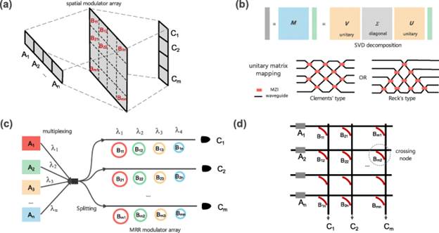
Optical vector matrix multipliers. a Vector matrix multiplier based on spatially separated devices. Ai, Bi, j and Ci represent input data, matrix element and computing result, respectively. b SVD decomposition. Here, V, Σ and U represent a unitary matrix, a diagonal matrix and a unitary matrix, respectively. Each unitary matrix can be uploaded into either Clement’s structure or Reck’s structure. c Scheme of VMM chip based on wavelength division multiplexing and micro-ring array. Ai, Bi, j and Ci represent input data, matrix element and computing result, respectively. d ‘Cross-bar’ scheme of VMM implemented by on-chip micro-comb and PCM modulator matrix. Ai, Bi, j and Ci represent input data, matrix element and computing result, respectively .
Moreover, benefiting from the quickly developed liquid-crystal-on-silicon (LCoS) technology and driving from the display industry, the resolution of SLM or DMD becomes fairly large (4 K resolution is commercially available). But the crosstalk error is the main obstacle to demonstrate the utmost performance of VMM employing high resolution SLM or DMD . Though the crosstalk issue could be circumvented by enlarging the pixel size of SLM or DMD, the functional area of SLM or DMD restricts the size of matrix. Meanwhile, the diffraction of light cannot be ignored even if using incoherent light source. This limitation is named as space–bandwidth product similar to the time-bandwidth product in the traditional communication system.
In recent years, many creative works have been proposed and demonstrated in waveguide rather than using traditional free-space VMM scheme. D. B. Miller has proposed a method to efficiently design an optical component for universal linear operation, which can be implemented by Mach-Zehnder interferometer (MZI) arrays. The basic idea is decomposing an arbitrary linear matrix into two unitary matrices and one diagonal matrix by using singular value decomposition (SVD) which can be easily realized by MZI arrays. Shen and Harris et al. . demonstrated a deep learning neural network utilizing a programmable nanophotonic processor chip. The chip consists of 56 MZIs and works as one optical interference unit (OIU) with 4 input ports and 4 output ports, shown as Fig. 1(b). In this work, two OIUs have been used to implement an effective arbitrary linear operator with 4*4 matrix size for inference process of ANNs, and a 76.7% correctness for vowel recognition is achieved compared with 91.7% in a digital computer. Later, Shen and Harris founded startup Lightelligence and Lightmatter respectively to promote this paperwork a step further toward to commercial applications . In 2020, Lightmatter published a board-device demo called ‘Mars’ on the HotChips 32 forum, which integrated an opt-electrical hybrid chip and other supporting electronic components . The hybrid chip contains a photonics core supporting the multiplication between a 64-length vector and 64*64 matrix. An ASIC chip utilizing14 nm processing technology has been externally integrated for mainly driving active devices in the photonic core. Besides the impressive scale of operating matrix in photonic core, a new technology of nano-optical-electro mechanical system (NOEMS) has been adopted to reduce the power consuming of holding the status of MZIs. Since the matrix’s updating rate is lower than vector’s inputting rate, the chip’s performance can be estimated from 0.4 TMAC/s to 4 TMAC/s depending on the refreshing frequency of weights.
Besides using MZI arrays with SVD method, there are other on chip architectures which can support the directly matrix loading. These architectures are similar to the systolic array in Google’s TPU (tensor processing unit) and ‘crossbar’ design in the computing-in-memory field . Varies types of modulators can substantially replace MZI to achieve multiplication in these architectures mentioned above. Here, the optical microring device is cited as a canonical example since its smaller footprint compared with MZI device. Several remarkable VMM works have demonstrated by combining the optical microring arrays with the WDM scheme . A typical scheme is shown in Fig. 1(c), the vector data is loaded on different wavelengths and the matrix is implemented by an optical microring array. The wavelength-selectivity of optical microring can eliminate the crosstalk of data with different wavelengths. Recently, a massively parallel convolution scheme based on a crossbar structure has been proposed and experimentally demonstrated by Feldmann et al.. In this work, a 16*16 ‘tensor core’ based on crossbar architecture has been built on chip. The optical crossbar has been implemented by using crossing waveguides and PCM modulators embedded in the coupled waveguide bends, as shown Fig. 1(d). Moreover, a chip-scale microcomb has been employed as the multi-wavelength light source. With the fixed matrix data and 13 GHz modulation speed of the input vector, the performance of this chip can reach more than 2 TMAC/s. Meanwhile, utilizing the PCM as a nonvolatile memory in computing is a wise approach for DNNs because the optical-electrical conversion overhead of weights data refreshing can be eliminated. Therefore the energy cost of system can be significantly reduce .