Producing Semiconductor-Grade Silicon
Introductory Remarks
|
Ø It is written somewhere that in the beginning God created heaven and the earth. It is not written from what. |
||
|
· We do not know for sure what the heaven is made of but we do know what the the earth is made of, at least as far as the upper crust is concerned. Interestingly enough, he (or she) created mostly Silicon and Oxygen with some dirt (in the form of the other 90 elements) thrown in for added value. |
||
|
· Indeed, the outer crust of this planet (lets say the first 100 km or so) consists of all kinds of silicates - Si + O + something else - so there is no lack of Si as a raw material. Si, in fact, accounts for about 26 % of the crust, while O weighs in at about 49 %. |
||
|
Ø However, it took a while to discover the element Si. Berzellius came up with some form of it in 1824 (probably amorphous), but it was Deville in 1854 who first obtained regular crystalline Si. |
||
|
· This is simply due to the very high chemical reactivity of Si. Pure Si (not protected by a thin layer of very stable SiO2 as all Si crystals and wafers are) will react with anything, and that creates one of the problems in making it and keeping it clean. |
||
|
· Liquid Si indeed does react with all substances known to man - it is an universal solvent. This makes crystal growth from liquid Si somewhat tricky, because how do you contain your liquid Si? Fortunately, some materials - especially SiO2 - dissolve only very slowly, so if you don't take too long in growing a crystal, they will do as a vessel for the liquid Si. |
||
|
· But there will always be some dissolved SiO2 and therefore oxygen in your liquid Si, and that makes it hard to produce Si crystals with very low oxygen concentrations. |
||
|
Ø What we need, of course, are Si crystals - in the form of wafers - with extreme degrees of perfection. |
||
|
· What we have are inexhaustible resources of Silicondioxide, SiO2, fairly clean, if obtained from the right source. Since there is no other material with properties so precisely matched to the needs of the semiconductor industry, and therefore of the utmost importance for our modern society, the production process of Si wafers shall be covered in a cursory way. |
||
|
|
||
|
Producing "Raw" Silicon |
||||
|
|
|
|||
|
Ø Fortunately, the steel industry needs Si, too. And Si was already used as a crucial alloying component of steel before it started its career as the paradigmatic material of our times. |
||||
|
· Most of the world production of raw Si still goes to the steel industry and only a small part is diverted for the semiconductor trade. This is why this stuff is commonly called "metallurgical grade" Si or MG-Si for short. The world production in 2006 was around 4 Mio tons per year. |
||||
|
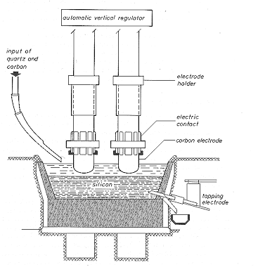
· How is MG- Si (meaning poly crystalline material with a purity of about 99%) made? More or less like most of the other metals: Reduce the oxide of the material in a furnace by providing some reducing agent and sufficient energy to achieve the necessary high temperatures.. |
||||
|
Ø Like for most metals, the reducing agent is carbon (in the form of coal or coke (= very clean coal)). The necessary energy is supplied electrically. |
||||
|
· Essentially, you have a huge furnace (lined with C which will turn into very hard and inert SiC anyway) with three big graphite electrodes inside (carrying a few 10.000 A of current) that is continuously filled with SiO2 (=quartz sand) and carbon (= coal) in the right weight relation plus a few added secret ingredients to avoid producing SiC. This looks like this |
||||
|
||||
|
· The chemical reaction that you want to take place at about 2000 oC is |
||||
|
||||
|
· But there are plenty of other reactions that may occur simultaneously, e.g. Si + C ⇒ SiC. This will not only reduce your yield of Si, but clog up your furnace because SiC is not liquid at the reaction temperature and extremely hard - your reactor ends up as a piece of junk if you make SiC. |
||||
|
Ø Still, we do not have to worry about MG-Si - a little bit of what is made for the steel industry will suffice for all of Si electronics applications. |
||||
|
· What we do have to do is to purify the MG-Si - about 109 fold! |
||||
|
Ø This is essentially done in three steps: |
||||
|
· First, Si is converted to SiHCl3 in a "fluid bed" reactor via the reaction |
||||
|
||||
|
Ø Second, the SiHCl3 is distilled (like wodka), resulting in extremely pure Trichlorosilane. |
||||
|
Ø Third, high-purity Si is produced by the Siemens process or, to use its modern name, by a "Chemical Vapor Deposition" (CVD) process - a process which we will encounter more often in the following chapters. |
||||
|
|
||||
|
Producing Doped Poly-Silicon |
||||
|
|
|
|||
|
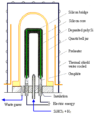
Ø The doped poly-Si (not to be confused with the poly-Si layers on chips) used for the growth of single Si crystals is made in a principally simple way which we will discuss by looking at a poly-Si CVD reactor |
||||
|
||||
|
· In principle, we have a vessel which can be evacuated and that contains an "U" shaped arrangements of slim Si rods which can be heated from an outside heating source and, as soon as the temperature is high enough (roughly 1000 oC) to provide sufficient conductivity, by passing an electrical current through it. |
||||
|
· After the vessel has been evacuated and the Si rods are at the reaction temperature, an optimized mix of SiHCl3 (Trichlorosilane), H2 and doping gases like AsH3 or PH3 are admitted into the reactor. In order to keep the pressure constant (at a typical value of some mbar), the reaction products (and unreacted gases) are pumped out at a suitable place. |
||||
|
· On hot surfaces - if everything is right this will only be the Si - a chemical reaction takes place, reducing the SiHCl3 to Si and forming HCl (hydrochloric acid) as a new compound: |
||||
|
||||
|
· Similar reactions provide very small but precisely measured amounts of As, P or B that will be incorporated into the growing polysilicon |
||||
|
· The Si formed will adhere to the Si already present - the thin rods will grow as fresh Si is produced. The incorporation of the dopants will produce doped polysilicon. |
||||
|
Ø In principle this is a simple process, like all CVD processes - but not in reality. Consider the complications: |
||||
|
· You have to keep the Si ultrapure - all materials (including the gases) must be specially selected. |
||||
|
· The chemistry is extremely dangerous: AsH3 and PH3 are among the most poisonous substances known to mankind; PH3 was actually used as a toxic gas in world war II with disastrous effects. H2 and SiHCl3 are easily combustible if not outright explosive, and HCl (in gaseous form) is even more dangerous than the liquid acid and extremely corrosive. Handling these chemicals, including the safe and environmentally sound disposal, is neither easy nor cheap. |
||||
|
· Precise control is not easy either. While the flux of H2 may be in the 100 liter/min range, the dopant gases only require ml/min. All flow values must be precisely controlled and, moreover, the mix must be homogeneous at the Si where the reaction takes place. |
||||
|
· The process is slow (about 1 kg/hr) and therefore expensive. You want to make sure that your hyperpure (and therefore expensive) gases are completely consumed in the reaction and not wasted in the exhaust - but you also want high throughput and good homogeneity; essentially conflicting requirements. There is a large amount of optimization required! |
||||
|
· And from somewhere you need the slim rods - already with the right doping. |
||||
|
Ø Still, it works and abut 10.000 tons of poly-Si are produced at present (2000) with this technology, which was pioneered by Siemens AG in the sixties for the microelectronic industry. (in 2007 it is more like 21.000 to plus another 30.000 tons for the solar industry). |
||||
|
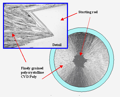
· Electronic grade Si is not cheap, however, and has no obvious potential to become very cheap either. The link provides todays specifications and some more information for the product. Here is an example for the poly-crystalline rods produced in the Siemens process: |
||||
|
||||
|
· While this is not extremely important for the microelectronics industry (where the added value of the chip by far surpasses the costs of the Si), it prevents other Si products, especially cheap solar cells (in connection with all the other expensive processes before and after the poly-Si process). Starting with the first oil crisis in 1976, many projects in the USA and Europe tried to come up with a cheaper source of high purity poly-Si, so far without much success. |
||||
|
· By now. i.e. in 2007, demand for electronic grade Si si surging because of a booming solar cell industry. |
||||