Functional Testing
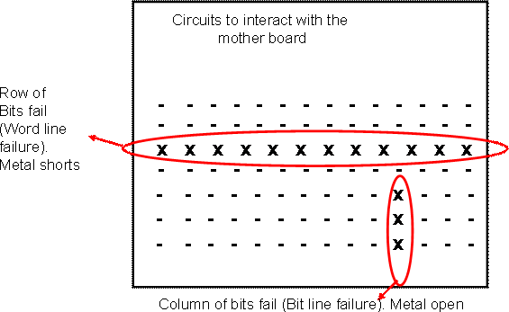
FBM: In the memory region, the
bits are arranged in rows and columns. If one or two bits fail randomly in a
chip, then it is difficult to identify the cause of the failure. However, if a
row of bits have failed, based on the design, the engineer will be able to
conclude that M1 line has shorted (as an example). If a column of bits have
failed, the engineer can conclude that a particular metal line is open (i.e.
the line is broken). The ‘row’s are called word lines and the
columns are called bit
lines as shown in the schematic (Fig. 10.5)

Fig 10.5. Schematic of a
fail bit map in a chip
If we find that in many chips, the ‘column failures’ are frequently observed, it is possible to conclude that the metal process is sub optimal and that it has to be improved. In other areas of the chip, such as the logic, the design is not repetitive. The design is complicated in those areas and it is not easy to identify the cause of failures in those regions.
Memory
Repair: In a memory chip, millions are bits are created and there
is a good chance that at least one of them may have a defect. A set of 1024
bits is called one kilobit, and a set of 1024 kilobits are called 1 megabit. If
one designs the memory with exactly the required number of bits, then it is
likely that at least 1 in 10 chips will have a failure. i.e. the yield will be
90%. However, most of the fabs achieve much more than 90% yield on a regular
basis, for the memory.
This is achieved by the following strategy. Instead of making exactly 1024 bits
(for example) in the design, the design will incorporate a few extra bits. If
any of the bits in the main array fail, then the connections to them is removed
by a laser. i.e. the lines connecting the bits will be melted (fused). The
lines connecting the extra bits will be left alone. The first test is
called “pre-fuse” test. If all the bits of the main array are created properly
and pass the ‘pre-fuse’ test, then the lines connecting the extra bits will be
disconnected using the laser. This is because the circuit should have the
exact number of bits and can’t have either shortage of bits or excess bits.
After fusing, the memory will be tested again (post-fuse test). The yield in
post-fuse testing is usually more than 95%. This process is called
‘repair’. If many bits in the memory part fail, then the chip cannot be
repaired. It is not worth adding many extra bits in the chip. Each bit
will occupy certain area, and adding too many extra bits will cause problem.
Thus, there is a balance between adding extra bits to enhance the memory yield
and occupying extra space.
A processor in the logic area will have very complicated structures and only
when the structures are very repetitive like memory, it is possible to have
excess bits and repair it. In the logic area, it is not possible to have backup
or redundant circuits. In few areas it may be possible to have a little
redundancy, but majority of the transistors will not be redundant and it will
not be possible to repair them.
High temperature
test: The chip will be subjected to high temperature and
tested. In case of military applications, the chip may be subjected to low
temperature and tested also. (e.g. the chips used in satellites or missiles will
have to encounter both high and low temperatures and hence these chips
should be tested at harsh conditions before they are packaged and used).
Optical
testing: The tests discussed above are called “electrical tests” since
they are based on electrical measurements. Other types of tests involve
electromagnetic waves. Although they used visible light waves many years ago,
the modern equipment also use electromagnetic waves in UV region. However, the
name ‘optical’ testing is applied for all these tests regardless of the
wavelength used. KLA-Tencor is a leading manufacturer of the
equipment used to identify the defects. They have a branch in India (as of
2011), to cater to the needs of semiconductor industry in south east asia.
The optical tests are used at various stages of processing, (i.e. before the
chip is completely fabricated). Specifically, they are used to determine if
there are any defects on the wafers. Defects may arise due to dust particles
falling on wafer, or due to poor process. For example, during CVD, dust
particles present in the chamber may fall on the wafer. If the dust particles
are observed frequently, then the CVD chamber must be cleaned before it is
used. In another example, during CMP, deep scratches may be formed on the wafer
due to large abrasive particles present in the slurry. In that case, the slurry
must be filtered so that only small abrasive particles are present.
The sizes of defects and dust particles that must be observed are very small
(< 100 nm). It must be noted that the features present in the chip, such as
interconnect copper lines, are also of similar size. Hence the equipment must
be capable of distinguishing between the desired features (such as interconnect
lines) and unwanted ones, such as dusts. If the circuits were simple, it
would be possible to compare the actual image with the ideal image (based on
the layout). However, in complicated circuits, it is not possible to load all
the layout details and compare with the image, in a short time. One way of
handling this is to image two neighboring chips simultaneously and compare
them. If both images are the same, then it can be assumed that there are no
defects. When they are different, the presence of defect can be
identified.