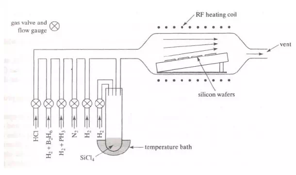
Epitaxial Growth
Epitaxy is used to deposit N on N+ silicon, which is impossible to accomplish by diffusion. It is also used in isolation between bipolar transistors wherein N- is deposited on P. We list below, and with reference to Figure, the sequence of operation involved in the process:
1. Heat wafer to 1200°C.
2. Turn on H2 to reduce the SiO2 on the wafer surface.
3. Turn on anhydrous HCl to vapor-etch the surface of the wafer.
This removes a small amount of silicon and other contaminants.
4. Turn off HCl.
5. Drop temperature to 1100°C.
6. Turn on silicon tetrachloride (SiCl4).
7. Introduce dopant.
Plasma- based ion implantation and film deposition system
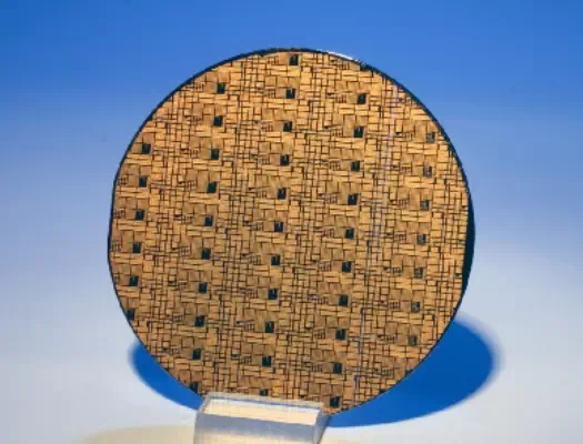
4" Wafer after Metallization
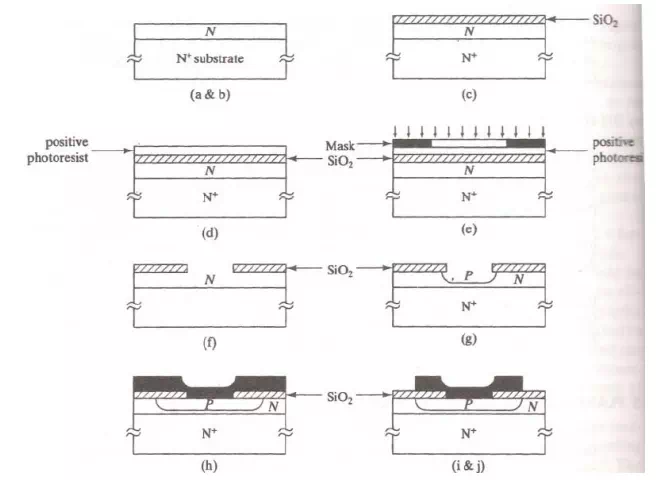
Planar PN Junction Diode Fabrication
Figure Process Description
1. An N+ substrate grown by the Czochralski process is the starting metal of approximatly 150 μm thick.
2. A layer of N-type silicon (1-5 μm) is grown on the substrate by epitaxy.
3. Silicon dioxide layer deposited by oxidation.
4. Surface is coated with photoresist (positive).
5. Mask is placed on surface of silicon, aligned, and exposed to UV light.
6. Mask is removed, resist is removed, and SiOz under the exposed resist is etched.
7. Boron is diffused to form P region. Boron diffuses easily in silicon but not in SiO 2
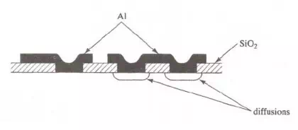
8. Thin aluminum film is deposited over surface.
9. Metallized area is covered with resist and another mask is used to identify areas where metal is to be preserved. Wafer is etched to remove unwanted metal. Resist is then dissolved.
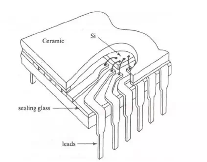
10. Contact metal is deposited on the back surface and ohmic contacts are made by heat treatment.