Common Source JFET Amplifier
Common Source JFET Amplifier uses junction field effect transistors as its main active device offering high input impedance characteristics
Transistor amplifier circuits such as the common emitter amplifier are made using Bipolar Transistors, but small signal amplifiers can also be made using Field Effect Transistors. These devices have the advantage over bipolar transistors of having an extremely high input impedance along with a low noise output making them ideal for use in amplifier circuits that have very small input signals. The design of an amplifier circuit based around a junction field effect transistor or “JFET”, (N-channel FET for this tutorial) or even a metal oxide silicon FET or “MOSFET” is exactly the same principle as that for the bipolar transistor circuit used for a Class A amplifier circuit we looked at in the previous tutorial. Firstly, a suitable quiescent point or “Q-point” needs to be found for the correct biasing of the JFET amplifier circuit with single amplifier configurations of Common-source (CS), Common-drain (CD) or Source-follower (SF) and the Common-gate (CG) available for most FET devices. These three JFET amplifier configurations correspond to the common-emitter, emitter-follower and the common-base configurations using bipolar transistors. In this tutorial about FET amplifiers we will look at the popular Common Source JFET Amplifier as this is the most widely used JFET amplifier design.
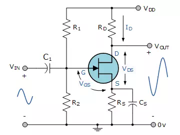
Consider the Common Source JFET Amplifier circuit configuration below.
Common Source JFET Amplifier
The amplifier circuit consists of an N-channel JFET, but the device could also be an equivalent N-channel depletion-mode MOSFET as the circuit diagram would be the same just a change in the FET, connected in a common source configuration. The JFET gate voltage Vg is biased through the potential divider network set up by resistors R1 and R2and is biased to operate within its saturation region which is equivalent to the active region of the bipolar junction transistor. Unlike a bipolar transistor circuit, the junction FET takes virtually no input gate current allowing the gate to be treated as an open circuit. Then no input characteristics curves are required. We can compare the JFET to the bipolar junction transistor (BJT) in the following table.
JFET to BJT Comparison
|
Junction FET |
Bipolar Transistor |
|
Gate, ( G ) |
Base, ( B ) |
|
Drain, ( D ) |
Collector, ( C ) |
|
Source, ( S ) |
Emitter, ( E ) |
|
Gate Supply, ( VG ) |
Base Supply, ( VB ) |
|
Drain Supply, ( VDD ) |
Collector Supply, ( VCC ) |
|
Drain Current, ( ID ) |
Collector Current, ( IC ) |
Since the N-Channel JFET is a depletion mode device and is normally “ON”, a negative gate voltage with respect to the source is required to modulate or control the drain current. This negative voltage can be provided by biasing from a separate power supply voltage or by a self biasing arrangement as long as a steady current flows through the JFET even when there is no input signal present and Vg maintains a reverse bias of the gate-source pn junction. In our simple example, the biasing is provided from a potential divider network allowing the input signal to produce a voltage fall at the gate as well as voltage rise at the gate with a sinusoidal signal. Any suitable pair of resistor values in the correct proportions would produce the correct biasing voltage so the DC gate biasing voltage Vg is given as:
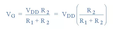
Note that this equation only determines the ratio of the resistors R1 and R2, but in order to take advantage of the very high input impedance of the JFET as well as reducing the power dissipation within the circuit, we need to make these resistor values as high as possible, with values in the order of 1MΩ to 10MΩ being common.
The input signal, (Vin) of the common source JFET amplifier is applied between the Gate terminal and the zero volts rail, (0v). With a constant value of gate voltage Vg applied the JFET operates within its “Ohmic region” acting like a linear resistive device. The drain circuit contains the load resistor, Rd. The output voltage, Vout is developed across this load resistance.
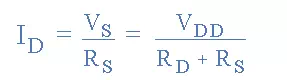
The efficiency of the common source JFET amplifier can be improved by the addition of a resistor, Rs included in the source lead with the same drain current flowing through this resistor. Resistor, Rs is also used to set the JFET amplifiers “Q-point”. When the JFET is switched fully “ON” a voltage drop equal to Rs*Id is developed across this resistor raising the potential of the source terminal above 0v or ground level. This voltage drop across Rs due to the drain current provides the necessary reverse biasing condition across the gate resistor, R2 effectively generating negative feedback. So in order to keep the gate-source junction reverse biased, the source voltage, Vs needs to be higher than the gate voltage, Vg. This source voltage is therefore given as:

Then the Drain current, Id is also equal to the Source current, Is as “No Current” enters the Gate terminal and this can be given as:
This potential divider biasing circuit improves the stability of the common source JFET amplifier circuit when being fed from a single DC supply compared to that of a fixed voltage biasing circuit. Both resistor, Rs and the source by-pass capacitor, Cs serve basically the same function as the emitter resistor and capacitor in the common emitter bipolar transistor amplifier circuit, namely to provide good stability and prevent a reduction in the loss of the voltage gain. However, the price paid for a stabilized quiescent gate voltage is that more of the supply voltage is dropped across Rs.
The the value in farads of the source by-pass capacitor is generally fairly high above 100uF and will be polarized. This gives the capacitor an impedance value much smaller, less than 10% of the transconductance, gm (the transfer coefficient representing gain) value of the device. At high frequencies the by-pass capacitor acts essentially as a short-circuit and the source will be effectively connected directly to ground. The basic circuit and characteristics of a Common Source JFET Amplifier are very similar to that of the common emitter amplifier. A DC load line is constructed by joining the two points relating to the drain current, Id and the supply voltage, Vdd remembering that when Id = 0: ( Vdd = Vds ) and when Vds = 0: ( Id = Vdd/RL ). The load line is therefore the intersection of the curves at the Q-point as follows.