IDEAL DIODE
The first electronic device to be introduced is called the diode. It is the simplest of semiconductor devices but plays a very vital role in electronic systems, having characteristics that closely match those of a simple switch. It will appear in a range of applications, extending from the simple to the very complex. In addition to the details of its construction and characteristics, the very important data and graphs to be found on specification sheets will also be covered to ensure an understanding of the terminology employed and to demonstrate the wealth of information typically available from manufacturers.
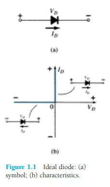
The term ideal will be used frequently in this text as new devices are introduced. It refers to any device or system that has ideal characteristics—perfect in every way. It provides a basis for comparison, and it reveals where improvements can still be made. The ideal diode is a two-terminal device having the symbol and characteristics shown in Figs. 1.1a and b, respectively.

Ideally, a diode will conduct current in the direction defined by the arrow in the symbol and act like an open circuit to any attempt to establish current in the opposite direction. In essence:
The characteristics of an ideal diode are those of a switch that can conduct current in only one direction.
In the description of the elements to follow, it is critical that the various letter symbols, voltage polarities, and current directions be defined. If the polarity of the applied voltage is consistent with that shown in Fig. 1.1a, the portion of the characteristics to be considered in Fig. 1.1b is to the right of the vertical axis. If a reverse voltage is applied, the characteristics to the left are pertinent. If the current through the diode has the direction indicated in Fig. 1.1a, the portion of the characteristics to be considered is above the horizontal axis, while a reversal in direction would require the use of the characteristics below the axis. For the majority of the device characteristics that appear in this book, the ordinate (or “y” axis) will be the current axis, while the abscissa (or “x” axis) will be the voltage axis.
One of the important parameters for the diode is the resistance at the point or region of operation. If we consider the conduction region defined by the direction of ID and polarity of VD in Fig. 1.1a (upper-right quadrant of Fig. 1.1b), we will find that the value of the forward resistance, RF, as defined by Ohm’s law is
![]()
where VF is the forward voltage across the diode and IF is the forward current through the diode.
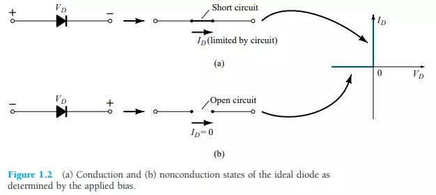
The ideal diode, therefore, is a short circuit for the region of conduction. Consider the region of negatively applied potential (third quadrant) of Fig. 1.1b

where VR is reverse voltage across the diode and IR is reverse current in the diode.
The ideal diode, therefore, is an open circuit in the region of nonconduction.
In review, the conditions depicted in Fig. 1.2 are applicable.

In general, it is relatively simple to determine whether a diode is in the region of conduction or nonconduction simply by noting the direction of the current ID established by an applied voltage. For conventional flow (opposite to that of electron flow), if the resultant diode current has the same direction as the arrowhead of the diode symbol, the diode is operating in the conducting region as depicted in Fig. 1.3a. If the resulting current has the opposite direction, as shown in Fig. 1.3b, the opencircuit equivalent is appropriate.

As indicated earlier, the primary purpose of this section is to introduce the characteristics of an ideal device for comparison with the characteristics of the commercial variety. As we progress through the next few sections, keep the following questions in mind:
· How close will the forward or “on” resistance of a practical diode compare with the desired 0-Ω level?
· Is the reverse-bias resistance sufficiently large to permit an open-circuit approximation?