Sinusoidal Inputs; Half-Wave Rectification
The diode analysis will now be expanded to include time-varying functions such as the sinusoidal waveform and the square wave. There is no question that the degree of difficulty will increase, but once a few fundamental maneuvers are understood, the analysis will be fairly direct and follow a common thread.
The simplest of networks to examine with a time-varying signal appears in Fig. 2.43. For the moment we will use the ideal model (note the absence of the Si or Ge label to denote ideal diode) to ensure that the approach is not clouded by additional mathematical complexity.
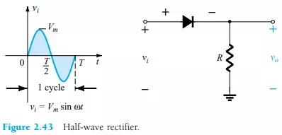
Over one full cycle, defined by the period T of Fig. 2.43, the average value (the algebraic sum of the areas above and below the axis) is zero. The circuit of Fig. 2.43, called a half-wave rectifier, will generate a waveform vo that will have an average value of particular, use in the ac-to-dc conversion process. When employed in the rectification process, a diode is typically referred to as a rectifier. Its power and current ratings are typically much higher than those of diodes employed in other applications, such as computers and communication systems.
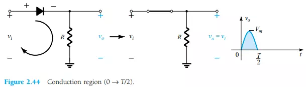
During the interval t = 0 → T/2 in Fig. 2.43 the polarity of the applied voltage vi is such as to establish “pressure” in the direction indicated and turn on the diode with the polarity appearing above the diode. Substituting the short-circuit equivalence for the ideal diode will result in the equivalent circuit of Fig. 2.44, where it is fairly obvious that the output signal is an exact replica of the applied signal. The two terminals defining the output voltage are connected directly to the applied signal via the short-circuit equivalence of the diode.
For the period T/2 → T, the polarity of the input vi is as shown in Fig. 2.45 and the resulting polarity across the ideal diode produces an “off” state with an open-circuit equivalent. The result is the absence of a path for charge to flow and vo = iR = (0)R = 0 V for the period T/2 → T. The input vi and the output vo were sketched together in Fig. 2.46 for comparison purposes. The output signal vo now has a net positive area above the axis over a full period and an average value determined by
![]()
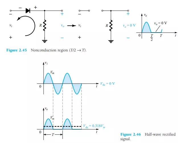
The process of removing one-half the input signal to establish a dc level is aptly called half-wave rectification.
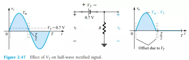
The effect of using a silicon diode with VT = 0.7 V is demonstrated in Fig. 2.47 for the forward-bias region. The applied signal must now be at least 0.7 V before the diode can turn “on.” For levels of vi less than 0.7 V, the diode is still in an opencircuit state and vo = 0 V as shown in the same figure. When conducting, the difference between vo and vi is a fixed level of VT = 0.7 V and vo = vi VT, as shown in the figure. The net effect is a reduction in area above the axis, which naturally reduces the resulting dc voltage level. For situations where Vm >> VT, Eq. 2.8 can be applied to determine the average value with a relatively high level of accuracy.
![]()
In fact, if Vm is sufficiently greater than VT, Eq. 2.7 is often applied as a first approximation for Vdc.
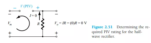
PIV (PRV)
The peak inverse voltage (PIV) [or PRV (peak reverse voltage)] rating of the diode is of primary importance in the design of rectification systems. Recall that it is the voltage rating that must not be exceeded in the reverse-bias region or the diode will enter the Zener avalanche region. The required PIV rating for the half-wave rectifier can be determined from Fig. 2.51, which displays the reverse-biased diode of Fig. 2.43 with maximum applied voltage. Applying Kirchhoff”s voltage law, it is fairly obvious that the PIV rating of the diode must equal or exceed the peak value of the applied voltage. Therefore,
![]()