PCB

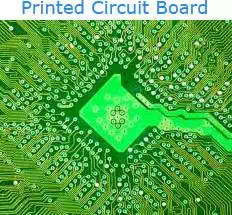
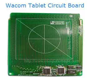
Sometimes abbreviated as a board, a PCB is short for printed circuit board and was invented by Paul Eisler while working on a radio in 1936. A PCB is made of plastic or fiberglass that holds ICsand other components. A good example of a PCB found in all computers today is the computer motherboard. The circuit board is most often green from the solder mask that coats the board, however, can be any other color, including red, blue, and even black. The picture is close-up of a printed circuit board. In the picture below, is an example of a circuit board from a Wacom tablet, in the bottom right portion of this board are some ICs that give the board its brains.

What is the biggest circuit board in a computer?
In a desktop computer, the motherboard is the largest circuit board that all other boards and devices connect to and communicate with each other.
What are the boards that connect to a motherboard?
In a desktop computer, expansion cards can be added to a computer to upgrade an existing component (e.g., a video card) or add new functionality to a computer.
Printed Circuit Board Definition & The History of the PCB
What is a PC board? When did printed circuit boards first come into usage?
We created this page to help define what printed circuit boards are and trace their history up to the present day. Printed circuit boards sure have come a long way since these early days in 1942. Today, Advanced Circuits manufactures printed circuit boards using the latest materials that allow electronic design engineers to miniaturize their products and build them to withstand demanding environments. To get where we are today as the nation’s third leading PCB manufacturer, with outstanding reliability and Exclusive Services (free PCB design layout software, PCB Artist and free file check, FreeDFM.com) there had to be an invention and history of the printed circuit board. We invite you to read about the origins of the PCB and how it has been used throughout the 20th and 21st centuries.
Printed Circuit Board Definition & History
To define what a PC board is, we have to look back at history that traces the evolution of printed circuit boards back to the early 20th century. The first PCB patents for "printed wire" were issued in the early 1900's but PCBs that we would recognize first came into use after World War II. In 1925, Charles Ducas of the United States submitted a patent application for a method of creating an electrical path directly on an insulated surface by printing through a stencil with electrically conductive inks. Hence the name "printed wiring" or "printed circuit." An Austrian scientist, Dr Paul Eisler, is credited with making the first operational printed wiring board in 1943. It was used as a replacement for bulky radio tube wiring.
PCB – Used in the 1920's
The earliest PCB's (printed circuit boards) were made from materials like Bakelite, Masonite, layered cardboard and even thin wooden planks. Holes were drilled into the material and then flat brass "wires" were riveted or bolted onto the board. Connections to components were usually made by pressing the end of the brass trace onto a hollow rivet and the component's leads were simply pressed into the open end of the rivet. Occasionally small nuts and bolts were used in place of the rivets. These types of PCBs were used in early tube style radios and gramophones in the 1920's.
By the 50's and early 60's laminates using different types of resins mixed with all sorts of different materials were being introduced but the pcbs were still single sided. The circuitry was on one side of the board and the components on the other. The advantages of the PCB over bulky wiring and cables made it a prime choice for new products being brought into the market place. But the largest influence on the evolution of the printed wiring board came from the government agencies responsible for new weapons and communication equipment. Wire ended components were being used in some of the applications. In the beginning the leads of the components were held in place on the board by using small nickel plates welded to the lead after it was placed through the hole.
PCB - The Evolution of the Production Process
Eventually processes were developed that would plate copper onto the walls of the drilled holes. That allowed circuits on both sides of the board to be connected electrically. Copper had replaced brass as the metal of choice because of its ability to carry electrical current, relatively low cost and ease of manufacturing. In 1956 the US Patent Office issued a patent for the "Process of Assembling Electrical Circuits" that was sought by a small group of scientists represented by the US Army. The patented process involved using a base material like melamine to which a layer of copper foil had been securely laminated. A drawing was made of the wiring pattern and then photographed onto a zinc plate. The plate was used to create a printing plate for an offset printing press. An acid resistant ink was printed onto the copper foil side of the board that was etched to remove the exposed copper leaving the "printed wire" behind. Other methods like using stencils, screening, hand printing and rubber stamping were also proposed to deposit the ink pattern. Holes were then punched in patterns using dies to match the position of the component wire leads or terminals. The leads were inserted through the non-plated holes in the laminate material and then the card was dipped or floated on a bath of molten solder. The solder would coat the traces as well as connecting the leads of the components to the traces.
They also used tinned eyelets, rivets and washers to attach various types of components to the board. Their patent even has a drawing showing two single sided boards stacked on top of each other with a standoff holding them apart. There are components on the top side of each board and one component shown with its leads extending through the top board into holes on the bottom board, connecting them together, a rough attempt at making the first multi-layer.
Much has changed since then. With the advent of plating processes that allowed hole walls to be plated came the first double sided boards. Surface mount pad technology, something we associate with the 1980's was actually being explored twenty years earlier in the 60's. Solder masks were being applied as early as 1950 to help reduce the corrosion that was occurring to traces and components. Epoxy compounds were spread over the surface of the assembled boards similar to what we know now as conformal coating. Eventually the inks were being screen printed onto the panels before assembling the boards. Areas that were meant to be soldered were blocked out on the screens. It helped keep the boards clean, reduce corrosion and oxidation but the tin/lead coating used to coat the traces would melt during the soldering process causing the mask to flake off. Because of the wide spacing of the traces it was seen more as a cosmetic problem than a functional issue. By the 1970's circuitry and spacing was becoming smaller and smaller and the tin/lead coating that was still being used to coat the traces on the boards began fusing traces together during the soldering process.
Hot air soldering methods began in the late 70's allowing the tin/lead to be stripped after etching eliminating the problem. Solder mask could then be applied over the bare copper circuits and leave only the plated holes and pads free to be coated with solder. As holes continued to get smaller and trace work became more densely packed solder mask bleed and registration issues brought on dry film masks. They were primarily used in the US while the first photo-imageable masks were being developed in Europe and Japan. In Europe the solvent based "Probimer" ink was applied by curtain coating the entire panel. The Japanese centered on screen processes using various aqueous developed LPIs. All of three of these mask types used standard UV exposure units and photo tools to define the pattern on the panel. By the mid 1990's the aqueous developed liquid photo-imageable masks were dominating the industry with specialized equipment designed specifically for their application.
The increased complexities and densities that were driving the evolution of solder mask were also forcing the development of layers of copper traces laminated between layers of dielectric materials. 1961 marked the first use of multi-layer pcbs in the United States. The development of the transistor and the miniaturization of other components drew more and more manufacturers into using printed circuit boards for an increasing number of consumer products. Aerospace equipment, flight instrumentation, computers and telecommunication products as well as defense systems and weapons all began to take advantage of the space saving that a multi-layer circuit board provided. Surface mount devices were being designed that wers wilenth the size and weight of the comparable through hole components. Followed by the invention of integrated circuits the circuit board has continued to shrink in almost every way. Rigid boards and cable applications have given way to flexible circuit boards or combinations of rigid and flexible PCBs. These and other advancements will keep the manufacture of printed circuit boards a dynamic field for many years.
Why is Solder Mask Green for PCB's?
Ever wonder why the solder mask on almost every circuit board made is green? Well there seems to be any number of unsubstantiated reasons. Everything from the involvement of the US government in developing and using the first circuit boards to the how easy it was on your eyes during the long hours of hand assembling the first boards.
Here's the most believable explanation I've heard. The original masks used a base resin that was a "brownish yellow" and a hardener that was a deeper muddy brown. When they were mixed together they created a honey brown color that apparently not very appetizing. They tried adding red pigments but it became a rusty adobe color and using blue simply made it a darker brown. None of them were very appealing colors. Since the laminate materials at the time had a green hue they tried adding more yellow and some blue and ended up with an acceptable green color. It became the standard color we are still using today.