Operational Amplifier Basics
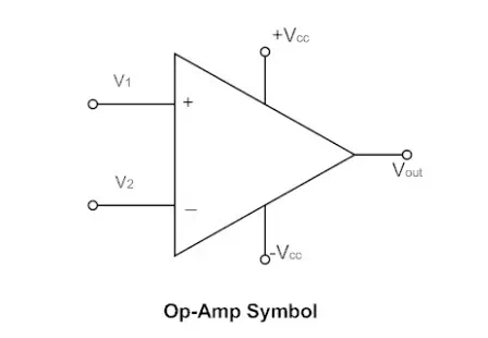
An operational amplifier commonly known as op-amp is a two-input single-output differential voltage amplifier which is characterized by high gain, high input impedance and low output impedance.
The operational amplifier is called so because it has its origins in analog computers, and was mainly used to perform mathematical operations. Depending on its feedback circuit and biasing, an op-amp can be made to add, subtract, multiply, divide, negate, and interestingly even perform calculus operations like differentiation and integration.
Today, op-amps are very popular building blocks in electronic circuits. Op-amps are used for a variety of applications such as AC and DC signal amplification, filters, oscillators, voltage regulators, comparators and in most of the consumer and industrial devices. Op-amps exhibit little dependence on temperature-changes or manufacturing variations, which makes them ideal building blocks in electronic circuits.
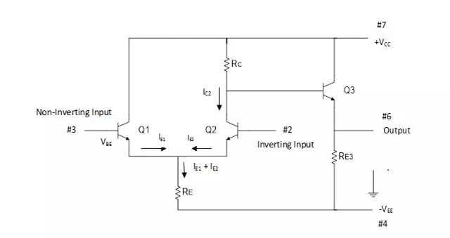
The basic circuit of an operational amplifier is as shown in the figure above. An op-amp has a differential amplifier input stage and emitter follower output stage. Practical op-amp circuits are much more complicated than the above shown basic op-amp circuit.
Transistors Q1 and Q2 forms a differential amplifier, where the difference input voltage is applied to the base terminals of Q1 and Q2. Transistor Q3 operates as an emitter follower and provides low output impedance.
The output of the basic op-amp circuit VOUT is given as,
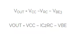
Where, VRC is the voltage across the resistor RC and VBE3 is the base-emitter voltage of transistor Q3.
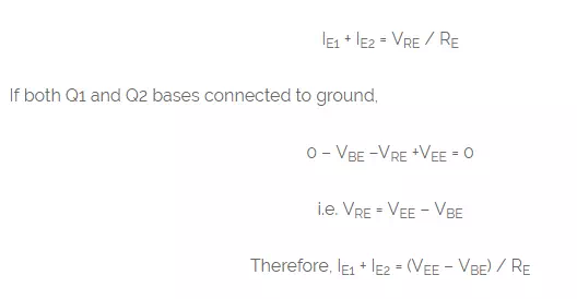
Assume that the transistors Q1 and Q2 are matched transistors i.e., they have equal VBE levels and equal current gains. If both transistors base terminals are connected to ground, the emitter currents IE1 and IE2 are equal and both IE1 and IE2 flow through the common resistor RE. The emitter current is given by the relation,
When a positive voltage is applied to the non-inverting input terminal, the base of Q1 is pulled up by the input voltage and its emitter terminal follows the input signal. Since Q1 and Q2 emitters are connected together, the emitter of Q2 also gets pulled up by the positive input at the non-inverting terminal. The base of Q2 is grounded, so the positive voltage at its emitter causes a reduction in its base-emitter voltage VBE2 . The reduction in VBE2 causes the emitter current IE2 to decrease and consequently IC2 also reduced.
t can be noted that a positive input at pin #3 gives a positive output, hence the name non-inverting input terminal.
Op-Amp Symbol
Note:
1. If an input signal is applied to either of the input terminals to the other input terminal connected to ground, the operation is called “single-ended”.
In single-ended operation a single input applied, drives both the transistors due to the common-emitter connection. The output obtained is thus driven by both the collectors.
2. If two input signals are applied to the two input terminals the operation is referred to as “double-ended”.
In double-ended operation the difference of the inputs applied to the two input terminals drives the transistors and the output obtained is driven by both the collectors.
If the same input is applied to both inputs, the operation is called “common mode”. In common-mode operation the common input signal at both the input terminals results in opposite signals at each collector. These signals get cancelled, resulting in an output signal zero. Practically, the opposite signals do not completely cancel each other and a small signal is resulted in the output.