Zener Diode I-V Characteristics Curve
In the forward bias condition, the zener diode behaves like an ideal diode within specified current and power limits, but it differs in reverse bias condition where the zener diode has very steep avalanche characteristic at the breakdown voltage in reverse bias condition.
Zener operates mainly in the reverse bias mode by connecting anode to the negative terminal of the power supply. Zener diodes are categorised and rated by the voltage at which they will turn on or start to conduct the reverse bias current.
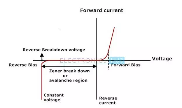
Generally these zener diodes are used to regulate the voltage. In reverse bias condition after the break down zener diode provides a constant output voltage even if we increase the input voltage. There are specifically two separate mechanisms that might cause a breakdown in a zener diode:
Avalanche Breakdown
It is predominant above approximately 5.5 volts. This mechanism is also referred to as impact ionisation or avalanche multiplication. For reverse conduction it is necessary to visualise the phenomenon of avalanche breakdown. This process begins when a large negative bias is applied to the PN junction, sufficient energy is imparted to thermally generated minority charge carriers in the semiconductors.
As a result the free carriers acquire required kinetic energy to break the covalent bonds and create an electric field through collisions with crystal particles. The charge carriers created in collision contribute to the reverse current, well beyond the normal reverse saturation current and may also possess enough energy to participate through collisions, creating an additional electric field and the avalanche effect by impact ionization, once a sufficiently high reverse bias is provided this process of conduction takes place very much like an avalanche: a single electron can ionise several others.
Zener Breakdown
It is predominant below approximately 5.5 volts. This mechanism is also referred to as a high field emission mechanism. The phenomenon of zener breakdown is related to the concept of avalanche breakdown. Zener breakdown is achieved by heavily doped regions in the neighbourhood of ohmic contact.
It is the second method of disturbing the covalent bonds of the crystal atoms and increasing the reverse bias zener diode current, to be sustained at a much lower specific voltage than normal diode. The reverse bias voltage known as zener voltage, where this mechanism occurs is determined by the diode doping concentration and it occurs when the depletion layer field width is sufficiently enough to disrupting the covalent bonds and cause number of free charge carriers due to electric field generation to swell.