Characteristics of a Signal Diode
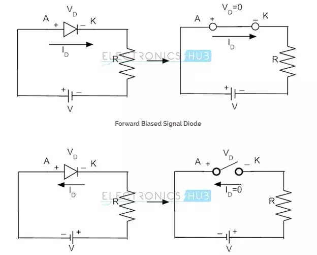
If both the positive and negative terminals of external power supply are connected to the respective terminals of the PN junction, then the signal diode is said to be in Forward Bias. The voltage supplied to the diode in forward bias generates a forward current denoted by IF. The value of forward current is directly proportional to the external voltage applied and reciprocally proportional to the inbuilt resistance of the diode.
The electrostatic force that prohibits the electrons and holes passing away from the junction due to the effect of charge ions within the depletion layer is named as barrier voltage. The typical values of barrier voltage at the p-n junction of germanium diode are 0.2 V ~ 0.3 V, whereas it is 0.6 V~ 0.7 V for silicon diode.
If the positive terminal of the supply is connected to cathode of the signal diode and negative terminal is connected to anode of the diode, then the signal diode is said to be in reverse bias. When an external voltage is applied to the diode in reverse bias, a small amount of current known as leakage current exists due to the minority charge carriers crossing the depletion layer and moving away from it. This leakage current is also termed as Reverse Saturation Current denoted by or which is independent of external voltage applied, but depends on the temperature of the device.
If the applied reverse bias voltage is very high, the minority charge carriers acquire enough energy to collide and split up the covalent bonds to generate a significant number of electron – hole pairs. The phenomenon of electron – hole pair generation is called as breakdown. The maximum reverse voltage applied to the diode before its breakdown condition can be referred as peak reverse voltage or peak inverse voltage.
In forward bias, signal diode acts as closed switch and thus short circuited for driving current solely in one direction (from the positive terminal to the negative terminal). In reverse bias, silicon diode acts as open switch and thus open circuited for blocking the current flowing in the diode. Silicon signal diodes act as rectifiers, switching circuits, limiting circuits and in clipping circuits for clipping the short duration waveforms.
Signal Diode Characteristics
The parameter details of the signal diode characteristics and specifications for signal diodes are given below.
Peak Inverse Voltage (PIV)
Peak Inverse Voltage parameter is defined as the maximum amount of voltage that can be applied to the diode in reverse direction. This peak voltage should not be exceeded because the voltage greater than this peak voltage may cause the device failure. It is also referred to as maximum reverse voltage and it is less than the avalanche breakdown condition of the diode in reverse bias characteristic. Typical values of peak inverse voltage may vary from a few volts to thousands of volts. In rectifier circuits with regards to amplitude, the peak inverse voltage is termed as the utmost negative value of the sine-wave surrounded by a cycle’s negative alternation.
Power Dissipation (PD)
Total power dissipation is defined as the maximum amount of power that will be dissipated at the PN junction signal diode during the conduction of current. The excess power will be dissipated in the form of heat. The forward resistance of signal diode is a dynamic property, it is very small and sometimes it is varied. In that condition the total power dissipated will be measured by multiplying the voltage applied to the diode and forward current flowing through the signal diode.
Forward Current (IF)
The forward current rating parameter of a signal diode is defined as the maximum amount of anode current that a signal diode can handle easily without damaging the device. If the current exceeds the forward current rating value, then the signal diode may get damaged at the junction due to thermal overload.
Operating Temperature (T)
The maximum operating temperature parameter of a signal diode is more often related to the total power dissipation and also related to the temperature of the PN junction. It is defined as the maximum temperature of the device at which maximum forward current is reached. Beyond this temperature value the device gets damaged and leads to failure of the device. The PN junction signal diode should be maintained at a temperature wherein the maximum forward current is achieved before it gets deteriorates.
Specifications of 1N4148 Signal Diode:
Here are some specifications of 1N4148 signal diode. They are as follows.
· Maximum repetitive reverse voltage = 100 V
· Average rectified forward current = 200 mA
· Maximum direct forward current = 300 mA
· Maximum forward voltage drop = 1.0 V at 10 mA.
· Non-repetitive peak forward surge current = 1.0 A (pulse width = 1 s)
· Total power dissipation = 500 mW
· Reverse recovery time < 4 ns
