Diode Characteristics
Diode Current Equation
PN junction diode is widely known for passing the electric current solely in one direction. The amount of current flowing through the PN junction diode greatly depends on the type of material used and also depends on the concentration of doping in the fabrication of PN diode.
The main reason for the flow of current is due to the generation or recombination of majority charge carriers in the structure of the PN junction diode.
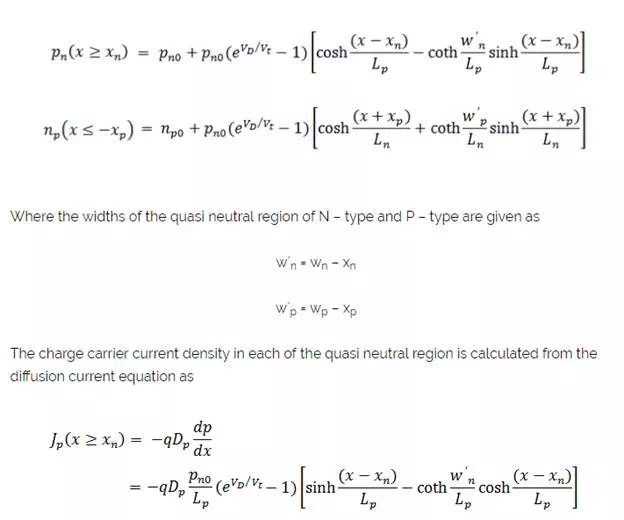
We will have three regions responsible for the flow of majority charge carrier current. These regions are namely quasi neutral P – region, depletion region, quasi neutral N – region. The region of the quasi neutral P – type is the separation between the edge of the depletion region and the edge of the diode on the P – side.
The region of the quasi neutral N – type is the separation between the edge of the depletion region and the edge of the diode on the N – side. For assumption, this separation distance is infinity. There will be no variation in the concentration of charge carriers as we move towards the boundaries of the diode. The electric field will not present in the quasi neutral region.
The diode current in the forward bias is due to the recombination of majority charge carriers. The charge carrier recombination takes place either in the P – type or N – type quasi neutral regions, in the depletion region or at the ohmic contacts i.e., at the contact of metal and semiconductor.
The current flow in the reverse bias is due to generation of charge carriers. This type of charge carrier generation process further increases the current flow in forward and also in reverse bias condition.
The flow of current in the PN junction diode is determined by the charge carrier density, the electric field throughout the structure of PN junction diode and the quasi Fermi level energies of the P – type and N – type. The carrier density and the electric field are used for determining the drift current and diffusion current of the PN diode.
The quasi Fermi level energies of the electrons and holes within the depletion region and that of in the N – type and P – type quasi neutral regions are assumed to be approximately equal in obtaining an analytical solution.
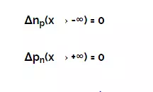
If the Fermi energy levels are assumed to be constant in the depletion region, the minority charge carrier density at the boundary of the depletion region would be as follows,
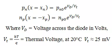
When there is no external voltage applied, thermal equilibrium state is reached at the above stated equations. The separation between the Fermi levels increases with the external applied voltage. This external voltage is multiplied by the charge of the electron.
The excess charge carriers present in either of the quasi region recombines straight away when they reach the metal – semiconductor contact. The process of recombination takes place rapidly at the ohmic contact and it further increases by the presence of metal. Therefore valid boundary conditions can be stated as follows,
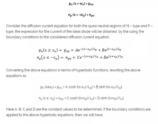
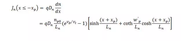
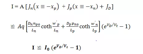
The amount of electric current flowing throughout the entire structure of the PN junction diode always should be constant, because no charge can disappear or accumulate in entire structure of diode.
Hence, total current through the diode is equal to the sum of the maximum hole current in the n-region, the maximum electron current in the p-region and the current because of the recombination of charge carriers in depletion region. The maximum currents in the quasi neutral regions occur at the sides of the depletion region.