Built in Potential
The majority charge carriers in the N-type region, i.e., electrons can cross the junction so as to recombine with majority charge carriers in the P-type region i.e. holes. As a result, a negative static space charge builds up in the P-type region as a result of the trivalent impurity boron atoms have a static negative charge as they unleash a positively-charged hole in the valence band. Whereas a positive space charge is formed in the N-type region for the similar reasons. The small volume where this space charge is created is referred to as the space charge zone or depletion zone. As there is a powerful electric field in this small volume, the density of free charge carriers is negligible at thermal equilibrium state.
If the P-type and N-type semiconductors are bringing nearer, a possible potential barrier is developed at the depletion layer. In fact, the static space charges are accumulated at the borders of the PN junction, positive charges in the N-type region and negative charges in the P-type region creates an electrical field ranging from N-type to P-type, that prevents diffusion and added recombination of electrons and holes. Diffusion is stopped by the formation of the internal electric field. As a result of the existence of this double layer of charges on either side of the PN junction, potential barrier varies sharply within the depletion zone and the potential difference Vd, called the diffusion potential or built-in potential reach non-negligible values. Electrostatic potential is constant all over the crystal together with the space charge zone, because this potential takes into consideration not only the electric field but also the concentration of charge carriers. The built in potential due to the concentration of charge carriers compensates accurately for the electrostatic potential.
The built-in potential or diffusion potential is proportional to the difference of the Fermi energies of the two unbounded semiconductors:
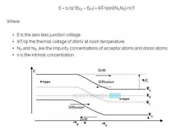
The built-in potential or junction potential of a semiconductor equals the potential across the depletion region in thermal equilibrium state. As the thermal equilibrium implies that the Fermi energy is constant throughout the PN diode device. The Fermi energies of the conduction band and valence band are therefore shifted up or down, and exhibit a sleek deviation across the region of depletion layer. As a result, there is an electrostatic potential energy difference showing between the P-type and N-type regions, equal to qVd.
The external potential needed to overcome the junction potential relies on the operating temperature and also the kind of semiconductor. Even if the external potential is not applied to the semiconductor, there exists some barrier potential due to electron-hole pair.
PN junction is formed on the single semiconductor and electrical contacts are laid around the semiconductor surface to enable the electrical connection for the external power supply. As a result of it the final device is termed as a PN junction diode or signal diode.