PN Junction
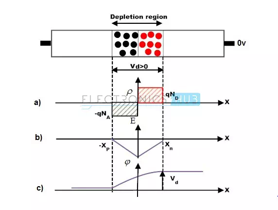
The PN junction is fabricated by sticking both the P-type and N-type within the same semiconductor crystal itself. The majority charge carriers in P-type is positively charged holes and in N-type is negatively charged electrons. The overall charge on both sides of a PN Junction must be equal and opposite to keep up a neutral charge condition around the junction owing to electron-hole pair. The layer between the P-type and N-type where the charge carriers are replicated multiple times is noted as depletion region.
In the equilibrium state no conduction takes place at the PN junction. The conduction of PN junction involves the majority charge carriers diffusion and minority charge carriers drift. Conduction of electrical current in PN junction physically involves in both conduction band and valence band. Once the external battery is provided the flow of electrons takes place in the conduction band, whereas the flow of holes takes place in the valence band.
At zero voltage bias equilibrium condition, the minority concentration of holes and electrons will drift simply under the influence of incorporating electric field E. The diffusion of majority charge carriers have to cross the potential barrier VB of the PN junction formed as the effect of the depletion region. This shall mean that majority charge carriers of the N-type and P-type should at least attain energy of qVB electron volts (eV) before it will surmount the barrier and diffuse into either P-type or N-type region. The shift of electrons from N side of the PN junction to holes annihilated on the P side of the PN junction produces a potential barrier voltage. The value of barrier voltage is close to 0.6 to 0.7 V in silicon, 0.3 V in germanium and varies with the levels of doping in different semiconductors.
The blocks of P-type and N-type semiconductors in contact with each other have no exploitable properties. Potential barrier must be crossed by the external voltage source to make the PN junction to conduct electricity. If a source of potential is connected in such a way that positive terminal is connected to P side and the negative terminal is connected to the N side. The negative terminal provides the electrons to the N-type to diffuse towards the depletion layer. Equally the positive terminal removes the electrons in the P-type creating holes that diffuse towards the depletion region. If the battery supply is big enough to overcome the barrier voltage, then the majority charge carriers from N-type and P-type combine and deplete the junction. As a result more number of charge carriers is replicated and flows towards the depletion region as long as the applied potential is greater than the potential barrier. Therefore majority charge current is conducted and flows towards the junction. During this approach once the current is conducted owing to majority charge carriers, the PN junction is said to be forward biased.
If the battery terminals are reversed, then the majority charge carriers of N-type are attracted by the positive terminal from the PN junction and the holes are attracted by the negative terminal far from the PN junction. The width of the depletion layer increases with the applied potential, as a result the recombination of charge carriers at the depletion layer do not takes place. Therefore, no conduction of electric current takes place. During this approach the PN junction is said to be reverse biased.