Channels and Banks
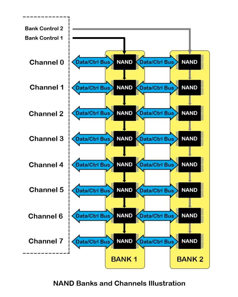
There is a control line which selects either Bank 1 or Bank 2 to be active on the Data/Control Bus for a specific channel. This control line is connected to the Chip Select of each NAND component to enable or disable the component.

NAND Channels:
Channels refer to the number of flash chips the controller can talk to simultaneously. Low end SSDs usually have 2 or 4 channels; high end SSDs usually have 8 channels, some have 10 channels.
SSD manufacturers can trade off performance vs power consumption by stuffing less channels at time of manufacture. The limitation on more channels is added die size, pin count and power consumption, which all increase the cost.
NAND Banks:
Each flash chip at the same location in a channel together constitutes a bank. Refer to the diagram above. Each channel can have multiple chips. The limitation on maximum number of chips is a result of pin count/die size/cost considerations.
Additional SSD Performance Techniques:

To further increase performance, controllers can take advantage of interleaving. Each NAND flash chip can have multiple dies in it, this is particularly so for high density parts. 2/4/8 die packs are common.
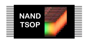
The illustration to the left shows a cutaway of a TSOP NAND component with multiple layers of die stacked on top of each other to create a single large capacity NAND flash chip.
For a multi-die package, it is possible for each die to carry out a command; this is refer to as interleaving and can significantly increase device performance. The ability to interleave is dependent on flash/controller/firmware support.
Another mechanism to improve performance is multi-plane operation. A flash chip is internally organized in planes, with low density devices being single plane and higher density devices with 2, 4 or more planes.
In a multi-plane devices, it is possible for all planes to carry out a command in parallel (this is like interleaving but for a single die). Multi-plane operation, when available, can substantially improve device performance.