How MLC and TLC store more than one bit per cell
The example above shows a SLC (Single Level Cell) NAND Cell. When any current is detected between the source and drain it can be concluded the cell is programmed. Since only two states, programmed or erased, are needed to represent one bit, that’s all that is needed.
With MLC (Multi Level Cell) NAND, there is a need to store two bits of data, which requires 4 distinct states. In order to accomplish this, the MLC NAND cell must be able to apply charge to the floating gate at four different levels and later be able to detect which of the four levels is set.
The diagram below represents the additional electrons in blue on the floating gate which must be set to precise levels so they can later be read accurately. This makes MLC more challenging and slower to write than their SLC NAND counterpart.
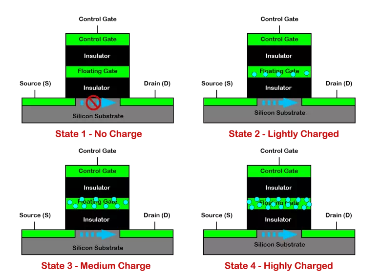
TLC (Tri Level Cell and also known as Triple Level Cell) NAND has an even more complicated mission. It must be able to store and recognize 3 bits per cell, requiring 8 distinct states.
Voltage Level in SLC, MLC and TLC NAND Cells:
The maximum voltage in each cell is about the same. So SLC cells have plenty of guard band between their states. Because of this, SLC NAND is able to withstand temperature extremes and other adverse effects much better than MLC or TLC NAND.
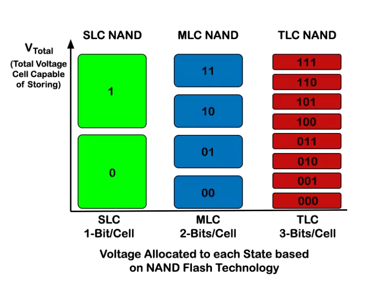
The Image above shows the levels of voltage thresholds required to store the multiple states in each of the memory technologies. Not counting guard band area, each SLC state is allocated 50% of the voltage range; MLC 25% and TLC 12.5%.
As you can see, MLC and TLC have much tighter tolerances and will be more susceptible than SLC NAND. Their principal advantage is cost.