Logic Gates
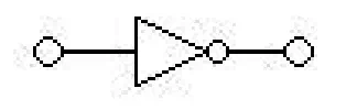
NOT
The simplest CMOS circuit: the NOT gate, or inverter. Although uncomplicated, it demonstrates the basic structure of a CMOS gate; a series of inputs (in this case, one) which are connected to the transistors, the PUN (consisting of a single p-type transistor) connected to source, the PDN (consisting of a single n-type transistor) connected to ground, and the output which is fed from both the PUN and PDN.
When the input voltage is high, the p-type transistor will be inactive, and the n-type transistor will be active. This creates a connection between ground and the gate output, pulling the gate’s output to low. Conversely, when the input voltage is low, the p-type transistor will be active instead, creating a connection between the output and source, pulling the gate’s output to high.

NAND
The PUN for NAND consists of a pair of p-type transistors in parallel, one with the A input feeding it and one with the B input feeding it. Therefore the PUN is active, and the output of the gate is high, as long as either of these inputs is low.
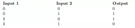
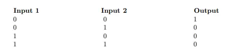
The PDN for NAND consists of a pair of n-type transistors in series, also each fed by one of the two inputs. Therefore the PDN is active, and the output of the gate is low, only if both of the inputs are high.it uses the logic a bar(OR)b bar.
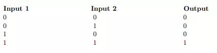
AND
A CMOS AND gate is constructed by driving a NOT gate from the output of a NAND gate.
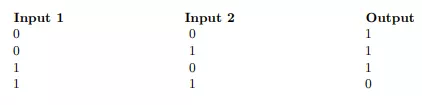
NOR
”Upside down” relative to the NAND gate, the NOR gate is made from a PUN of two p-type transistors in series and a PDN of two n-type transistors in parallel.
OR
As AND is to NAND, OR is to NOR. CMOS OR is constructed by feeding the output of NOR to a NOT gate.
XNOR
To build an XNOR gate, first we will need easy access to the inverted inputs. This is accomplished with a pair of NOT gates. The original inputs are A and B, and their inverted forms we will call NOT-A and NOT-B. Both the PUN and PDN are made of four of the appropriate type of transistor, in two parallel sets, of series of two transistors each. In the PUN there is one series fed by A and B and the other is fed by NOT-A and NOT-B; in the PDN one series is fed by A and NOT-B and the other is fed by NOT-A and B.
All told, this takes 12 transistors (4 in the PUN, 4 in the PDN, and 2 for each inverter). There are more efficient designs for the XNOR circuit, but they require a more detailed analysis than we will go into here. Instead of serving as an example of an actual XNOR design, this section should instead help to suggest the methods one could use to generate a CMOS circuit for any arbitrary Boolean function.

XOR
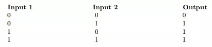
If you’ve been following along, you may guess that an XOR gate is made by attaching a NOT onto the end of the XNOR; while this will produce a correct circuit, it is not the most correct (or efficient) circuit. Instead, we could use the same 12 transistors and simply shuffle around the wires. This is left as an exercise for the reader. it uses the logic a.bbar(OR)abar.b