MOS implementation

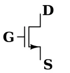
Since it is possible to use a MOSFET transistor as a voltage-controlled resistor, we can use this feature to create an analog multiplier. Let us refer to picture on the right. With the letter we indicate the different pins: D rain, S ource and G ate. MOS are symmetrical devices, so we could replace the drain with the source without affecting the behaviour of the device. Anyway we’ll call source the lowest voltage pin and drain the point with the highest voltage. When the voltage between gate and source is less than the voltage between drain and source, i.e. VGS < VDS, the relationship between current and voltage is the following:
![]()
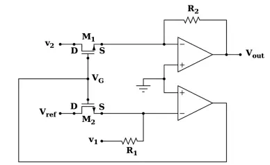
assuming we can always use this relationship, the analog multiplier configuration is the following:

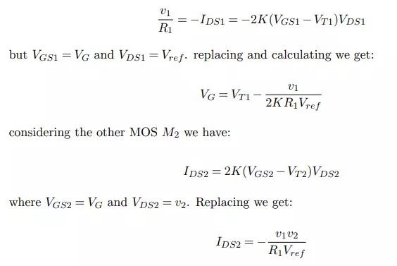
where source and drain of both devices are pointed out. If v2 and Vref are positive, then the sources will remain there because that points are virtually connected to ground by the operational amplifiers. The current flowing through R1 is defined: one side of the resistor has the voltage v1, the other one is grounded. That same current will flow through the MOS M1, thus defining the voltage VG. The current is given by:

from which we finally get the output voltage:

and this is what we wanted. The difference between the previous configurations are:
· the MOS implementation is simpler and requires fewer devices
· in the calculations for the diode configuration we did not introduce any approximation, while the MOS configuration we did.
In other words, the diode implementation is more complicated, but it works fine for a wider range on inputs.