Working under Reverse Biased
When an external voltage is applied to a diode such that it increases the potential barrier and restricts the flow of current is called as Reverse bias. When anode and cathode are connected to negative and positive terminals respectively, the electrons are attracted towards the positive terminal and holes are attracted towards the negative terminal. Hence both will be away from the potential barrier increasing the junction resistance and preventing any electron to cross the junction.
The following figure explains this. The graph of conduction when no field is applied and when some external field is applied are also drawn.
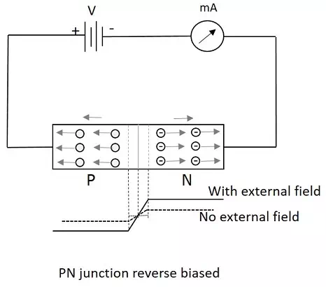
With the increasing reverse bias, the junction has few minority carriers to cross the junction. This current is normally negligible. This reverse current is almost constant when the temperature is constant. But when this reverse voltage increases further, then a point called reverse breakdown occurs, where an avalanche of current flows through the junction. This high reverse current damages the device.
Reverse current
Reverse current is the current produced by the diode when operating in reverse biased condition and it is indicated by Ir. Hence a diode provides high resistance path in reverse biased condition and doesn’t conduct, where it provides a low resistance path in forward biased condition and conducts. Thus we can conclude that a diode is a one-way device which conducts in forward bias and acts as an insulator in reverse bias. This behavior makes it work as a rectifier, which converts AC to DC.
Peak Inverse Voltage
Peak Inverse Voltage is shortly called as PIV. It states the maximum voltage applied in reverse bias. The Peak Inverse Voltage can be defined as “The maximum reverse voltage that a diode can withstand without being destroyed”. Hence, this voltage is considered during reverse biased condition. It denotes how a diode can be safely operated in reverse bias.