Working of N - Channel (depletion mode) MOSFET
For now, we have an idea that there is no PN junction present between gate and channel in this, unlike a FET. We can also observe that, the diffused channel N (between two N+ regions), the insulating dielectric SiO2 and the aluminum metal layer of the gate together form a parallel plate capacitor.
If the NMOS has to be worked in depletion mode, the gate terminal should be at negative potential while drain is at positive potential, as shown in the following figure.
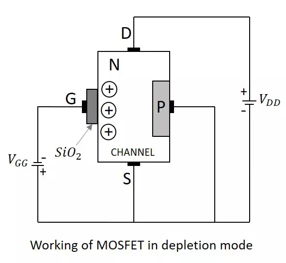
When no voltage is applied between gate and source, some current flows due to the voltage between drain and source. Let some negative voltage is applied at VGG. Then the minority carriers i.e. holes, get attracted and settle near SiO2 layer. But the majority carriers, i.e., electrons get repelled.
With some amount of negative potential at VGG a certain amount of drain current ID flows through source to drain. When this negative potential is further increased, the electrons get depleted and the current ID decreases. Hence the more negative the applied VGG, the lesser the value of drain current ID will be.
The channel nearer to drain gets more depleted than at source (like in FET) and the current flow decreases due to this effect. Hence it is called as depletion mode MOSFET.