Construction of N- Channel MOSFET
Let us consider an N-channel MOSFET to understand its working. A lightly doped P-type substrate is taken into which two heavily doped N-type regions are diffused, which act as source and drain. Between these two N+ regions, there occurs diffusion to form an Nchannel, connecting drain and source.
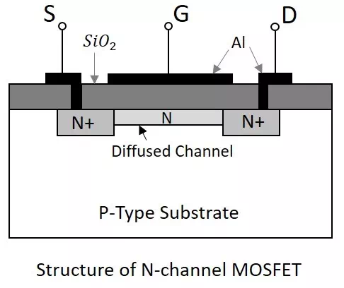
A thin layer of Silicon dioxide (SiO2) is grown over the entire surface and holes are made to draw ohmic contacts for drain and source terminals. A conducting layer of aluminum is laid over the entire channel, upon this SiO2 layer from source to drain which constitutes the gate. The SiO2substrate is connected to the common or ground terminals.
Because of its construction, the MOSFET has a very less chip area than BJT, which is 5% of the occupancy when compared to bipolar junction transistor. This device can be operated in modes. They are depletion and enhancement modes. Let us try to get into the details.