Drain Characteristics of JFET
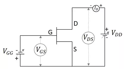
Let us try to summarize the function of FET through which we can obtain the characteristic curve for drain of FET. The circuit of FET to obtain these characteristics is given below.
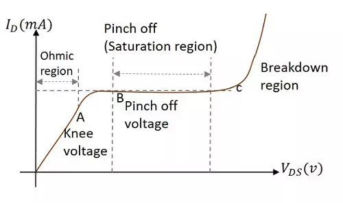
When the voltage between gate and source VGS is zero, or they are shorted, the current ID from source to drain is also nil as there is no VDSapplied. As the voltage between drain and source VDS is increased, the current flow ID from source to drain increases. This increase in current is linear up to a certain point A, known as Knee Voltage.
The gate terminals will be under reverse biased condition and as IDincreases, the depletion regions tend to constrict. This constriction is unequal in length making these regions come closer at drain and farther at drain, which leads to pinch off voltage. The pinch off voltage is defined as the minimum drain to source voltage where the drain current approaches a constant value (saturation value). The point at which this pinch off voltage occurs is called as Pinch off point, denoted as B.
As VDS is further increased, the channel resistance also increases in such a way that ID practically remains constant. The region BC is known as saturation region or amplifier region. All these along with the points A, B and C are plotted in the graph below.
The drain characteristics are plotted for drain current ID against drain source voltage VDS for different values of gate source voltage VGS. The overall drain characteristics for such various input voltages is as given under.
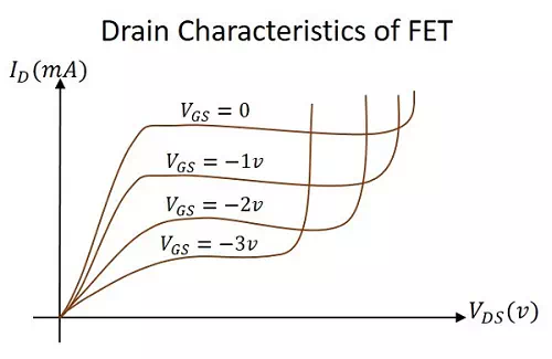
As the negative gate voltage controls the drain current, FET is called as a Voltage controlled device. The drain characteristics indicate the performance of a FET. The drain characteristics plotted above are used to obtain the values of Drain resistance, Transconductance and Amplification Factor.