Common Emitter (CE) Configuration
The name itself implies that the Emitter terminal is taken as common terminal for both input and output of the transistor. The common emitter connection for both NPN and PNP transistors is as shown in the following figure.
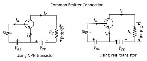
Just as in CB configuration, the emitter junction is forward biased and the collector junction is reverse biased. The flow of electrons is controlled in the same manner. The input current is the base current IB and the output current is the collector current IC here.
Base Current Amplification factor (β)
The ratio of change in collector current (ΔICΔIC) to the change in base current (ΔIBΔIB) is known as Base Current Amplification Factor. It is denoted by β
β=ΔICΔIBβ=ΔICΔIB
Relation between β and α
Let us try to derive the relation between base current amplification factor and emitter current amplification factor.
β=ΔICΔIBβ=ΔICΔIB
α=ΔICΔIEα=ΔICΔIE
IE=IB+ICIE=IB+IC
ΔIE=ΔIB+ΔICΔIE=ΔIB+ΔIC
ΔIB=ΔIE−ΔICΔIB=ΔIE−ΔIC
We can write
β=ΔICΔIE−ΔICβ=ΔICΔIE−ΔIC
Dividing by $$
β=ΔICΔIEΔIEΔIE−ΔICΔIEβ=ΔICΔIEΔIEΔIE−ΔICΔIE
α=ΔICΔIEα=ΔICΔIE
We have
α=ΔICΔIEα=ΔICΔIE
Therefore,
β=α1−αβ=α1−α
From the above equation, it is evident that, as α approaches 1, β reaches infinity.
Hence, the current gain in Common Emitter connection is very high. This is the reason this circuit connection is mostly used in all transistor applications.
Expression for Collector Current
In the Common Emitter configuration, IB is the input current and IC is the output current.
We know
IE=IB+ICIE=IB+IC
And
IC=αIE+ICBOIC=αIE+ICBO
=α(IB+IC)+ICBO=α(IB+IC)+ICBO
IC(1−α)=αIB+ICBOIC(1−α)=αIB+ICBO
IC=α1−αIB+11−αICBOIC=α1−αIB+11−αICBO
If base circuit is open, i.e. if IB = 0,
The collector emitter current with base open is ICEO
ICEO=11−αICBOICEO=11−αICBO
Substituting the value of this in the previous equation, we get
IC=α1−αIB+ICEOIC=α1−αIB+ICEO
IC=βIB+ICEOIC=βIB+ICEO
Hence the equation for collector current is obtained.
Knee Voltage
In CE configuration, by keeping the base current IB constant, if VCE is varied, IC increases nearly to 1v of VCE and stays constant thereafter. This value of VCE up to which collector current IC changes with VCE is called the Knee Voltage. The transistors while operating in CE configuration, they are operated above this knee voltage.
Characteristics of CE Configuration
· This configuration provides good current gain and voltage gain.
· Keeping VCE constant, with a small increase in VBE the base current IB increases rapidly than in CB configurations.
· For any value of VCE above knee voltage, IC is approximately equal to βIB.
· The input resistance ri is the ratio of change in base emitter voltage (ΔVBEΔVBE) to the change in base current (ΔIBΔIB) at constant collector emitter voltage VCE.
ri=ΔVBEΔIBatconstantVCEri=ΔVBEΔIBatconstantVCE
· As the input resistance is of very low value, a small value of VBE is enough to produce a large current flow of base current IB.
· The output resistance ro is the ratio of change in collector emitter voltage (ΔVCEΔVCE) to the change in collector current (ΔICΔIC) at constant IB.
ro=ΔVCEΔICatconstantIBro=ΔVCEΔICatconstantIB
· As the output resistance of CE circuit is less than that of CB circuit.
· This configuration is usually used for bias stabilization methods and audio frequency applications.