Transistor Configurations
A Transistor has 3 terminals, the emitter, the base and the collector. Using these 3 terminals the transistor can be connected in a circuit with one terminal common to both input and output in a 3 different possible configurations.
The three types of configurations are Common Base, Common Emitterand Common Collector configurations. In every configuration, the emitter junction is forward biased and the collector junction is reverse biased.
Common Base (CB) Configuration
The name itself implies that the Base terminal is taken as common terminal for both input and output of the transistor. The common base connection for both NPN and PNP transistors is as shown in the following figure.
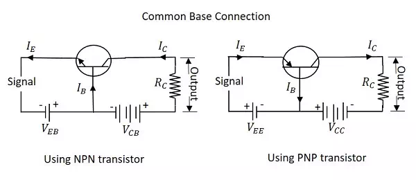
For the sake of understanding, let us consider NPN transistor in CB configuration. When the emitter voltage is applied, as it is forward biased, the electrons from the negative terminal repel the emitter electrons and current flows through the emitter and base to the collector to contribute collector current. The collector voltage VCB is kept constant throughout this.
In the CB configuration, the input current is the emitter current IE and the output current is the collector current IC.
Current Amplification Factor (α)
The ratio of change in collector current (ΔICΔIC) to the change in emitter current (ΔIEΔIE) when collector voltage VCB is kept constant, is called as Current amplification factor. It is denoted by α.
α=ΔICΔIEatconstantVCBα=ΔICΔIEatconstantVCB
Expression for Collector current
With the idea above, let us try to draw some expression for collector current. Along with the emitter current flowing, there is some amount of base current IB which flows through the base terminal due to electron hole recombination. As collector-base junction is reverse biased, there is another current which is flown due to minority charge carriers. This is the leakage current which can be understood as Ileakage. This is due to minority charge carriers and hence very small.
The emitter current that reaches the collector terminal is
αIEαIE
Total collector current
IC=αIE+IleakageIC=αIE+Ileakage
If the emitter-base voltage VEB = 0, even then, there flows a small leakage current, which can be termed as ICBO (collector-base current with output open).
The collector current therefore can be expressed as
IC=αIE+ICBOIC=αIE+ICBO
IE=IC+IBIE=IC+IB
IC=α(IC+IB)+ICBOIC=α(IC+IB)+ICBO
IC(1−α)=αIB+ICBOIC(1−α)=αIB+ICBO
IC=(α1−α)IB+(ICBO1−α)IC=(α1−α)IB+(ICBO1−α)
IC=(α1−α)IB+(11−α)ICBOIC=(α1−α)IB+(11−α)ICBO
Hence the above derived is the expression for collector current. The value of collector current depends on base current and leakage current along with the current amplification factor of that transistor in use.
Characteristics of CB configuration
· This configuration provides voltage gain but no current gain.
· Being VCB constant, with a small increase in the Emitter-base voltage VEB, Emitter current IE gets increased.
· Emitter Current IE is independent of Collector voltage VCB.
· Collector Voltage VCB can affect the collector current IC only at low voltages, when VEB is kept constant.
· The input resistance ri is the ratio of change in emitter-base voltage (ΔVEBΔVEB) to the change in emitter current (ΔIEΔIE) at constant collector base voltage VCB.
η=ΔVEBΔIEatconstantVCBη=ΔVEBΔIEatconstantVCB
· As the input resistance is of very low value, a small value of VEB is enough to produce a large current flow of emitter current IE.
· The output resistance ro is the ratio of change in the collector base voltage (ΔVCBΔVCB) to the change in collector current (ΔICΔIC) at constant emitter current IE.
ro=ΔVCBΔICatconstantlEro=ΔVCBΔICatconstantlE
· As the output resistance is of very high value, a large change in VCBproduces a very little change in collector current IC.
· This Configuration provides good stability against increase in temperature.
· The CB configuration is used for high frequency applications.