Operation PNP Transistor
The operation of a PNP transistor can be explained by having a look at the following figure, in which emitter-base junction is forward biased and collector-base junction is reverse biased.
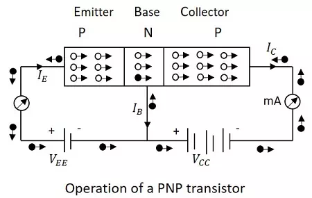
The voltage VEE provides a positive potential at the emitter which repels the holes in the P-type material and these holes cross the emitter-base junction, to reach the base region. There a very low percent of holes recombine with free electrons of N-region. This provides very low current which constitutes the base current IB. The remaining holes cross the collector-base junction, to constitute collector current IC, which is the hole current.
As a hole reaches the collector terminal, an electron from the battery negative terminal fills the space in the collector. This flow slowly increases and the electron minority current flows through the emitter, where each electron entering the positive terminal of VEE, is replaced by a hole by moving towards the emitter junction. This constitutes emitter current IE.
Hence we can understand that −
- The conduction in a PNP transistor takes place through holes.
- The collector current is slightly less than the emitter current.
- The increase or decrease in the emitter current affects the collector current.