Transistor Biasing
As we know that a transistor is a combination of two diodes, we have two junctions here. As one junction is between the emitter and base, that is called as Emitter-Base junction and likewise, the other is Collector-Base junction.
Biasing is controlling the operation of the circuit by providing power supply. The function of both the PN junctions is controlled by providing bias to the circuit through some dc supply. The figure below shows how a transistor is biased.
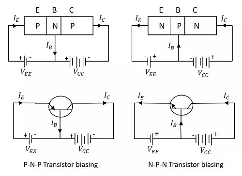
By having a look at the above figure, it is understood that
· The N-type material is provided negative supply and P-type material is given positive supply to make the circuit Forward bias.
· The N-type material is provided positive supply and P-type material is given negative supply to make the circuit Reverse bias.
By applying the power, the emitter base junction is always forward biased as the emitter resistance is very small. The collector base junction is reverse biased and its resistance is a bit higher. A small forward bias is sufficient at the emitter junction whereas a high reverse bias has to be applied at the collector junction.
The direction of current indicated in the circuits above, also called as the Conventional Current, is the movement of hole current which is opposite to the electron current.