Photo Diode
Photo diode, as the name implies, is a PN junction which works on light. The intensity of light affects the level of conduction in this diode. The photo diode has a P type material and an N-type material with an intrinsicmaterial or a depletion region in between.
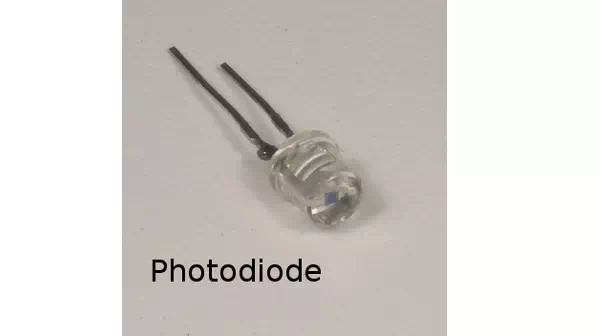
This diode is generally operated in reverse bias condition. The light when focused on the depletion region, electron-hole pairs are formed and flow of electron occurs. This conduction of electrons depends upon the intensity of light focused. The figure below shows a practical Photo diode.

The figure below indicates the symbol for a photodiode.

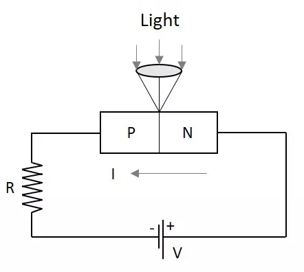
When the diode is connected in reverse bias, a small reverse saturation current flows due to thermally generated electron hole pairs. As the current in reverse bias flows due to minority carriers, the output voltage depends upon this reverse current. As the light intensity focused on the junction increases, the current flow due to minority carriers increase. The following figure shows the basic biasing arrangement of a photo diode.

The Photo diode is encapsulated in a glass package to allow the light to fall onto it. In order to focus the light exactly on the depletion region of the diode, a lens is placed above the junction, just as illustrated above.
Even when there is no light, a small amount of current flows which is termed as Dark Current. By changing the illumination level, reverse current can be changed.
Advantages of Photo diode
Photo diode has many advantages such as −
- Low noise
- High gain
- High speed operation
- High sensitivity to light
- Low cost
- Small size
- Long lifetime
Applications of Photo diode
There are many applications for photo diode such as −
- Character detection
- Objects can be detected (visible or invisible).
- Used in circuits that require high stability and speed.
- Used in Demodulation
- Used in switching circuits
- Used in Encoders
- Used in optical communication equipment
Another diode of such a kind is Solar cell. It is termed as a cell though it is a diode. Let us get into the details.