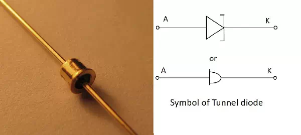
Tunnel diode
If the impurity concentration of a normal PN junction is highly increased, this Tunnel diode is formed. It is also known as Esaki diode, after its inventor.
When the impurity concentration in a diode increases, the width of depletion region decreases, extending some extra force to the charge carriers to cross the junction. When this concentration is further increased, due to less width of the depletion region and the increased energy of the charge carriers, they penetrate through the potential barrier, instead of climbing over it. This penetration can be understood as Tunneling and hence the name, Tunnel diode.
The Tunnel diodes are low power devices and should be handled with care as they easily get affected by heat and static electricity. The Tunnel diode has specific V-I characteristics which explain their working. Let us have a look at the graph below.
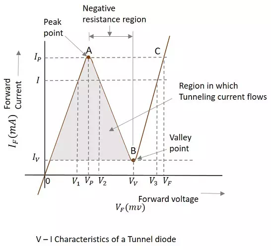
Consider the diode is in forward-biased condition. As forward voltage increases, the current increases rapidly and it increases until a peak point, called as Peak Current, denoted by IP. The voltage at this point is called as Peak Voltage, denoted by VP. This point is indicated by A in the above graph.
If the voltage is further increased beyond VP, then the current starts decreasing. It decreases until a point, called as Valley Current, denoted by IV. The voltage at this point is called as Valley Voltage, denoted by VV. This point is indicated by B in the above graph.
If the voltage is increased further, the current increases as in a normal diode. For larger values of forward voltage, the current increases further beyond.
If we consider the diode is in reverse-biased condition, then the diode acts as an excellent conductor as the reverse voltage increases. The diode here acts as in a negative resistance region.
Applications of Tunnel diode
There are many applications for tunnel diode such as −
- Used as a high-Speed Switching device
- Used as a memory storage device
- Used in Microwave oscillators
- Used in relaxation oscillators