Biasing of JFET
Different types of techniques are used to bias the JFET in a proper manner. From various techniques, below three are widely used:
§ Fixed DC Biasing Technique
§ Self-Biasing Technique
§ Potential Divider Biasing
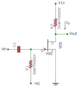
Fixed DC Biasing Technique
In fixed DC biasing technique of an N channel JFET, the gate of the JFET is connected in such a way that the VGS of the JFET remains negative all the time. As the input impedance of a JFET is very high there are no loading effects observed in the input signal. The current flow through the resistor R1 remains zero. When we apply an AC signal across the input capacitor C1, the signal appears across the gate. Now, if we calculate the voltage drop across the R1, as per the Ohms law it will be V = I x R or Vdrop = Gate current x R1. As the current flowing to the gate is 0 the Voltage drop across the gate remains zero. So, by this biasing technique, we can control the JFET drain current by just changing the fixed voltage thus changing the VGS.
Self-Biasing Technique
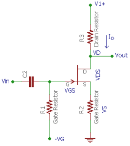
In self-biasing technique, a single resistor is added across the source pin. The voltage drop across the source resistor R2 creates the VGS to bias the voltage. In this technique, the gate current is zero again. The source voltage is determined by the same ohms law V = I x R. Therefore source voltage = Drain current x source resistor. Now, the gate to source voltage can be determined by the differences between gate voltage and source voltage.
Since the gate voltage is 0 (as the gate current flow is 0, as per V = IR, gate voltage = Gate current x gate resistor = 0 ) the VGS = 0 – Gate current x Source resistance. Thus there is no external biasing source is needed. The biasing is created by self, using the voltage drop across source resistor.
Potential Divider Biasing
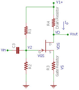
In this technique, an additional resistor is used and the circuit is slightly modified from the self-biasing technique, a potential voltage divider using R1 and R2 provide the required DC biasing for the JFET. The voltage drop across the source resistor is needed to be larger than the resistor divider gate voltage. In such a way the VGS remain negative.