Processing of Semiconductor Materials
Preparation of Silicon and Germanium – Silicon is one of the commonest elements on earth. It occurs as silicon dioxide (SiO2) and as silicates; mixtures of silicon and other materials. Germanium is derived from zinc or copper ores. When converted to bulk metal, silicon and germanium contain large quantities of impurities. Both metals must be carefully refined before they can be used for semiconductor device manufacture. Processing of Semiconductor Materials is normally polycrystalline after it is refined. This means that it is made up of many individual formations of atoms with no overall fixed pattern. For use in semiconductors, the metal must be converted into single-crystal material; that is, all of its atoms must be arranged into a single pattern.

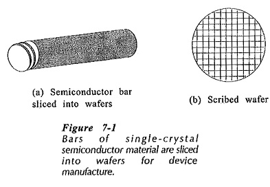
In its final condition for device manufacture, silicon and germanium are in the form of single-crystal bars about 2.5 cm in diameter and perhaps 30 cm long. The bars are sliced into disc-shaped wafers about 0.4 cm thick, and the wafers are polished to a mirror surface. Several thousand devices are usually fabricated on the surface of each wafer, then the wafers are scribed and cut like glass, (see Fig. 7-1)
Diffusion:
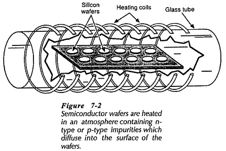
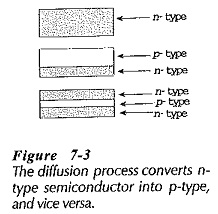
For processing, semiconductor wafers contained in an enclosure are heated by means of radio frequency (RF) heating coils. This is illustrated in Fig. 7-2. When wafers of n-type material are raised to a high temperature in an atmosphere containing p-type impurity atoms some of the impurities diffuse into each wafer. This converts the outer layer of the n-type material into p-type, (Fig 7-3). The diffusion process can be continued by further heating the wafers in an atmosphere containing n-type impurity atoms, so that npn layers are produced, as illustrated. Because the diffusion process is very slow (about 2.5 μm per hour), very narrow diffused regions can be created by careful timing.
Epitaxial Growth:
The epitaxial process is very similar to the diffusion process, except that silicon or germanium atoms are contained in the gas surrounding the semiconductor wafers.
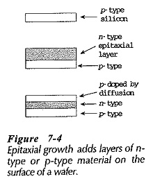
The semiconductor atoms in the gas grow (accumulate) on the wafer in the form of a thin layer, (Fig. 7-4). This layer is single-crystal material and it may be p-type or n-type, according to the impurity content of the gas. The epitaxial layer may be doped by the diffusion process.