Difference Between Common Base Common Emitter and Common Collector
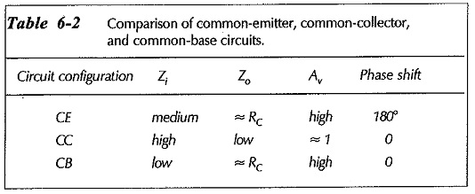
Table 6-2 compares Zi, Zo, and Av, for difference Between Common Base Common Emitter and Common Collector circuits. As already discussed, the CE circuit has high voltage gain, medium input impedance, high output impedance, and a 180° phase shift from input to output. The CC circuit has high input impedance, low output impedance, a voltage gain of 1, and no phase shift. The CB circuit offers low input impedance, high output impedance, high voltage gain, and no phase shift.
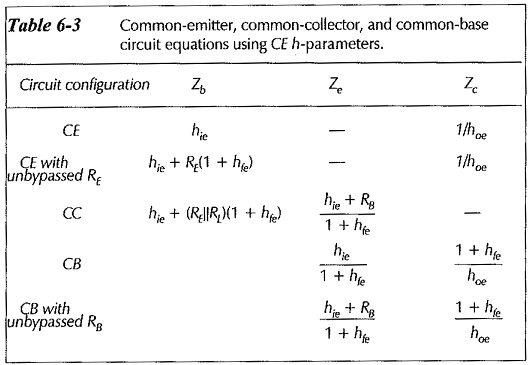
Device manufacturers normally only list the CE h-parameters on a transistor data sheet. Although these can be converted to CC and CB parameters, it is convenient to use CE parameters for all three types of circuits. Table 6-3 gives the circuit impedance equations in terms of CE h-parameters. In the case of input and output impedances, it is helpful to think in terms of the terminal being looked into.
Impedance at the Transistor Base:
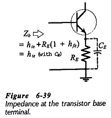
Consideration of each type of circuit shows that the input impedance (Zi) depends upon which transistor terminal is involved. In both the CE and CC circuits, the input signal is applied to the transistor base terminal. So, Zi is the impedance ‘looking into’ the base. Figure 6-39 shows that, for a CE circuit with an unbypassed emitter resistor,

When RE is bypassed, the RE(1 + hfe) portion can be treated as zero, so that,

The CC equations for Zb are almost identical to the CE equations, except that they use hic and hfc, which are essentially equal to hie and hfe, (see Table 6-3). A rough approximation for the base input impedance of any transistor circuit with an unbypassed emitter resistor is,

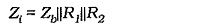
The circuit input impedance for both CE and CC configurations is Zb in parallel with the bias resistors,
Impedance at the Transistor Emitter:
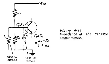
The transistor emitter is the output terminal for a CC circuit and the input terminal for a CB circuit. So, the device impedance in each case is the impedance ‘looking into’ the transistor emitter terminal (Ze). Although the Ze equations for the two circuits look different, they can be shown to give exactly the same result in similar situations. For a CC circuit or a CB circuit with an unbypassed base (using CE parameters),

where RB is the impedance ‘looking back’ from the transistor base.
As shown in Fig. 6-40, RB includes the signal source resistance (rs) for a CC circuit. A CB circuit normally has its base bypassed as shown, so that the impedance at the emitter is,

For all circuit arrangements, the impedance at the transistor emitter terminal is,
Impedance at the Transistor Collector:
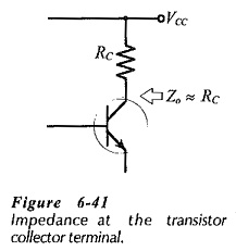
The output for CE and CB circuits is produced at the transistor collector terminal. So, the impedance ‘looking into’ the collector is the device output impedance. This is normally a very large quantity at low and medium signal frequencies. As illustrated in Fig. 6-41, the circuit output impedance at the collector is essentially,

Voltage gain:
In the case of a circuit with an unbypassed emitter resistor, the ac voltage at the emitter follows the ac input at the transistor base. So, a CC circuit (an emitter follower) has a voltage gain of 1.

With both CE and CB circuits, the ac input (vi) is developed across the base-emitter junction, and the ac output (vo) is produced at the transistor collector terminal, (see Fig 6-42). Thus, the magnitude of the voltage gain is the same for CB and CE circuits with similar component values and transistor parameters. The CE voltage gain equation can be used for the CB circuit, with the omission of the minus sign that indicates CE phase inversion.
Although the voltages gains are equal for similar CB and CE circuits, the low input impedance of the CB circuit can substantially attenuate the signal voltage, and result in a low amplitude output.