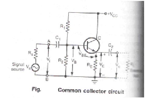
Common Collector Amplifier Circuit
From above circuit, D.C. biasing is provided by R1, R2 and RE. The load resistance is capacitor coupled to the emitter terminal of the transistor. When a signal is applied to base of the transistor, VB is increased and decreased as the signal goes positive and negative respectively.
From figure, VE = VB - VBE
Consider VBE is constant, so the variation in VB appears at emitter and emitter voltage VE will vary same as base voltage VB. In common collector circuit, emitter terminal follows the signal voltage applied to the base. It is also known as emitter follower.