Miller effect
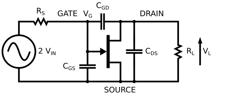
Mr. Miller was taking about vacuum tubes in his seminal paper, but the concept applies to all three-terminal amplifier devices. In terms of a more modern microwave field-effect transistor (FET), the Miller effect is an increase of the apparent gate to drain capacitance compared to the real one due to a feedback effect from the drain to the gate.
The gate to source capacitance, Cgs, sees at its terminals only the gate voltage, Vg. The drain to source capacitance, Cds, sees at its terminals the the drain voltage, vl. The drain voltage is basically the gate voltage multiplied by the voltage gain (hey, why do you think it was called an amplifier?) And the gate to drain capacitor sees at its terminals the gate voltage multiplied by (1+A), A being the voltage current of the device in the schematic below. The voltage current being a direct function of the output load. And since the gate to drain capacitor sees a multiplied voltage, its effect is multiplied by the same factor.
"Thus the apparent input capacity can become a number of times greater than the actual capacities between the tube electrodes ..." see page 374 in Miller's original article.
This increase of the apparent capacitance is problematic in broad-band circuits because the bandwidth is reduced when the capacitance increases. In narrowband circuits, the Miller effect is less of a problem because capacitance can always be compensated for by the inductance of the bias circuits. However, keep in mind that the bandwidth of a circuit must be sufficient to keep a margin for process variations.
Some remedies to this problems are :
- Put in parallel to the gate to drain capacitor an inductor to resonate the capacitor. But this compensation has some serious drawbacks. It is narrow-band. Nasty oscillations can occur. Yikes ! And the inductor must be DC-decoupled by a capacitor, because gate and drain bias voltages are different. Double trouble!
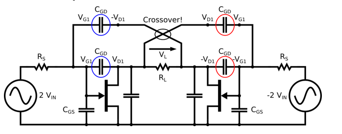
- Use a balanced amplifier and compensate Cgd by another capacitor of the same value connected to the opposite voltage, like explained in following picture. We let the derivation to the reader. However, two problems limits that cool scheme. First, oscillation can occur. Second, the layout needs an RF-RF cross-over, which is not practical.
-
- Decrease the load impedance seen by the transistor, to reduce the voltage gain. Remember that Miller effect is an effect of the voltage gain. Two schemes for that are the cascode and the Cherry-Hooper amplifier.
The cascode
The image below illustrates a common way to alleviate the Miller effect: the cascode. The load impedance seen by the first transistor is dramatically reduced by the second transistor. In such a configuration, the voltage gain of the first transistor is approximately 1. [Recall that both transistors are of the same kind, and that RS = 1 / gm.]. Since the voltage gain is low, the Miller effect is drastically reduced.
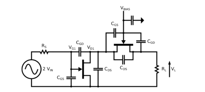
The second transistor has voltage gain but no current gain. And the Miller effect is eliminated because the gate is grounded for high frequencies. This scheme is usable only up to ft, not fmax. In general, ft is lower than fmax, at least for FET transistors. This should be kept in mind when designing really high frequency amplifiers, for example in the millimeter wave range.
Also, an other problem of this scheme is an huge tendency to oscillate. A damping RC network is almost always added to the gate of the second transistor stage to compensate for this problem.
Finally, the DC power consumption of the whole amplifier is doubled. Each transistor has a similar VDS voltage across it and the same current flowing into it. Additionally, for low voltage circuits, this scheme doubles the needed bias voltage so it's problematic. Lot of solutions have been developed to solve this problem but, hey, it's not an IEEE article here