Amplifier frequency response
INTRODUCTION
As
such for any electronic circuit, the behavior of
amplifiers is affected by the frequency of the signal on their input terminal.
This characteristic is known as the frequency response.
Frequency
response is one of the most important property of
amplifiers. In the frequency range that amplifiers have been designed for, they
must deliver a constant and acceptable level of gain. The frequency response
depends directly on the components and the architecture chosen for the design
of the amplifier.
In
this tutorial, we will focus on this important feature of amplifiers. First of
all, the notion of frequency response is detailed along with some basic related
concepts and we will present how to quantify it. In the second section, we will
understand which component affects the frequency response and how. In the rest
of the article a method to establish the low and high frequency responses is
presented. These results will finally be synthesized in the conclusion to plot
the global frequency response of a Common Emitter Amplifier.
DEFINITIONS
Before
defining in details the frequency response, we need to present the unit of
decibel (dB) and the logarithmic scale related to it. When studying the
frequency response, it is indeed more suitable to convert either the power or
voltage gain into dB and to represent the frequency scale in a logarithmic
(log) scale.
If
we consider an amplifier with power gain AP and voltage gain AV,
the power and voltage gain in dB are defined by :
eq 1 : Power and voltage gain in dB
While
the gains in linear scale are always positive (AP,AV≥0),
their equivalent in dB can either be positive if an amplification is being
realized (AP,AV>1) or negative if the input signal is attenuated
(AP,AV<1).
Often,
it is not the gain AV(dB) that is
investigated but rather a normalized ratio AV/AV,mid(dB)=20log(AV/AV,mid). Where AV,mid is
called the midrange gain and represents the maximum gain of the
amplifier in its frequency working range, for example 20 Hz – 20 kHz for an
audio amplifier.
Therefore,
when AV=AV,mid, the
normalized gain (written indifferently AV) is AV(dB)=0. This sets a 0 dB
reference when the gain is maximum. It is important to
note that when the power is divided by two, we observe that AP(dB)=10log(0.5)=-3 dB.
The
frequency at which the power drops to 50 % of its midrange value is known as
the cutoff frequency and noted fc.
Each time that the power is halved, a reduction of 3 dB of the normalized gain
is observed. Therefore AP=-3 dB corresponds to AV,mid/2, AP=-6 dB corresponds to AV,mid/4 and so on …
For
this same frequency, the voltage (or current) is multiplied by a factor √2=0.7.
Halving the voltage signal corresponds to a reduction of 6 dB and follows the
same pattern as presented for the power gain.
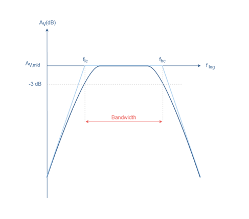
The
most common tool used to represent the frequency response of any system is
the Bode plot. It consists of the normalized gain AV(dB)
as a function of the frequency in log scale. A simplified Bode graph of an
amplifier is shown in the Figure 1 below :
fig
1 : Typical Bode graph of an amplifier
The
light blue curve is called the asymptotic representation while the dark blue
curve is the real frequency response of the circuit.
In Figure
1, two different cutoff frequencies can be distinguished : flc for
“low cutoff” and fhc for
“high cutoff”. The quantity fhc-flc is
called the bandwidth and represents the frequency range where the
gain is above the -3 dB plateau.
One
last observation can be given about the slope of the frequency response out of
the bandwidth. First of all, they are not necessary identical for low and high
frequencies. Moreover, as we will see later, the slope has a value that depends
on the reactance of the components that induce a dependency with the frequency.
EFFECT OF THE CAPACITORS
Let’s
consider a Common Emitter Amplifier (CEA) which configuration is
shown in Figure 2 :
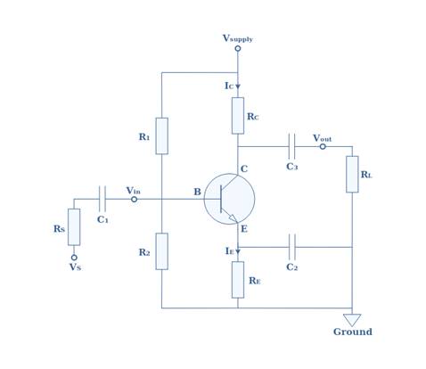
fig
2 : Common Emitter Amplifier
The
structure around the BJT transistor consists of a voltage divider network
(R1 and R2), a load (RL), coupling capacitors (C1 and C3) and a
bypass capacitor C2.
What
is important to keep in mind is that capacitors have a property
called reactance that is an equivalent of the resistance. The
reactance (XC) of capacitors depends on the frequency and the value of the
capacitor, it satisfies the following formula :
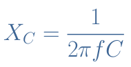
eq 2 : Reactance of capacitors
Independently
of the value of the capacitor, when the frequency is low, XC tends to be
high. Near DC signals, capacitors behave therefore as open circuits. On the
other hand, when the frequency increases XC tends to zero and capacitors
act as short circuits.
At
low input frequencies, the coupling capacitors will more likely block the
signal, since XC1 and XC3 are higher, more voltage drop will be
observed across C1 and C3. This results in a lower voltage gain.
At
high input frequencies the bypass capacitor C2 shortens the emitter branch
to the ground and the voltage gain of the amplifier is AV=(RC//RL)/re with re being the small diode emitter
resistance. When the frequencies are lower, the resistance between the emitter
and the ground is no longer only re but RE+re and
therefore the voltage gain decreases to AV=(RC//RL)/(RE+re).
There
is another type of capacitors that affect the frequency response of the
amplifier and is not represented in Figure 2. They are known
as internal transistor capacitors and represented in Figure
3 below :
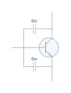
fig
3 : Internal transistor capacitors
Whereas
the coupling and bypass capacitors act as high-pass filter (they
block low frequencies), these internal capacitors behave differently. Indeed,
if the frequency is low, CBC and CBE act as an open circuit
and the transistor is not affected at all. However, if the frequency increases,
more signal passes through them instead of going in
the base branch of the transistor, therefore decreasing the voltage gain.
A
very important formula is given in Equation 3 and links the cutoff frequency of a RC filter :
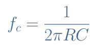
eq 3 : Cutoff frequency of a
RC filter
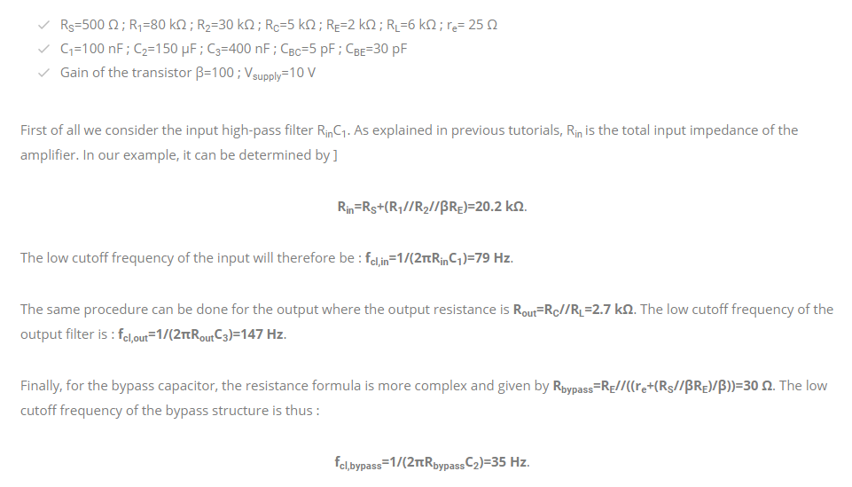
LOW FREQUENCY RESPONSE
Having
all of this information in mind, let’s calculate and plot the low frequency
response of the CEA of Figure 2 with the below given parameters :
One last thing we need to understand
before plotting the Bode graph is about the slope out of the midrange values.
The decrease of AV,mid with
the frequency is called roll-off and its value for each simple
RC filter is -20 dB/decade (dB/dec). This value means
for high-pass filters (resp. low-pass filters) that each time the frequency is
divided by 10 (resp. multiplied by 10), a decrease of -20 dB is observed for
the gain of the amplifier.
When multiple filters are blocking the same range of
frequencies, the roll-off is enhanced. In our example three filters are
simultaneously blocking the frequencies below 35 Hz, the roll-off is therefore
3*(-20 dB/dec)=-60 dB/dec.
This information can be synthesized in a Bode plot
showing the low frequency response of the CEA in asymptotic representation
:
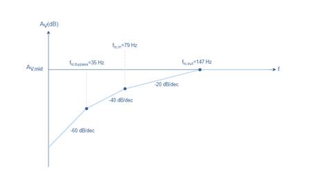
fig
4 : Low frequency response of the CEA