The Basic MOSFET Differential Pair
Differential or Single-Ended?
Introductory studies of active circuits generally devote a significant amount of time to standard single-ended amplifier configurations—e.g., common-source, common-gate, emitter-follower. This is certainly a worthy endeavor in the context of becoming familiar with transistor operation, small-signal analysis, and amplifier characteristics. But the practical value of single-ended amplifier configurations is a different story—the fact is, differential amplifiers dominate modern analog ICs. There are a few reasons for this:
![]() Differential
amplifiers apply gain not to one input signal but to the difference between
two input signals. This means that a differential amplifier naturally
eliminates noise or interference that is present in both input signals.
Differential
amplifiers apply gain not to one input signal but to the difference between
two input signals. This means that a differential amplifier naturally
eliminates noise or interference that is present in both input signals.
![]() Differential
amplification also suppresses common-mode signals—in other words, a DC offset
that is present in both input signals will be removed, and the gain will be
applied only to the signal of interest (assuming, of course, that the signal of
interest is not present in both inputs). This is particularly advantageous in
the context of IC design because it eliminates the need for bulky
DC-blocking capacitors.
Differential
amplification also suppresses common-mode signals—in other words, a DC offset
that is present in both input signals will be removed, and the gain will be
applied only to the signal of interest (assuming, of course, that the signal of
interest is not present in both inputs). This is particularly advantageous in
the context of IC design because it eliminates the need for bulky
DC-blocking capacitors.
![]() The
subtraction that occurs in a differential pair makes it easy to incorporate the
circuit into a negative-feedback amplifier, and if you’ve read the Negative
Feedback series, you know that negative feedback is about the best thing that
could ever happen to an amplifier circuit.
The
subtraction that occurs in a differential pair makes it easy to incorporate the
circuit into a negative-feedback amplifier, and if you’ve read the Negative
Feedback series, you know that negative feedback is about the best thing that
could ever happen to an amplifier circuit.
![]() It
is only sensible to expect these benefits to be accompanied by significant
disadvantages, but the nature of IC fabrication has rendered the differential
configuration almost wholly beneficial. Two concerns are 1) higher component
count and 2) the importance of symmetrical component characteristics. You can
forget about number 1 because the cost of adding a few more transistors to an
IC is negligible. As for number 2, IC technology happens to be very good at
achieving consistency among the components within a chip (this consistency is referred
to as “matching”).
It
is only sensible to expect these benefits to be accompanied by significant
disadvantages, but the nature of IC fabrication has rendered the differential
configuration almost wholly beneficial. Two concerns are 1) higher component
count and 2) the importance of symmetrical component characteristics. You can
forget about number 1 because the cost of adding a few more transistors to an
IC is negligible. As for number 2, IC technology happens to be very good at
achieving consistency among the components within a chip (this consistency is referred
to as “matching”).
![]() In
this article, we will explore the basic MOSFET differential-amplifier
configuration by means of conceptual discussion and simulations (i.e., not too
much math or complicated circuit analysis). Because this topic is relevant primarily
to IC implementation, we will use an NMOS model that is specific to 0.35 µm
CMOS technology; the various LTspice files and some related information can be
found here.
In
this article, we will explore the basic MOSFET differential-amplifier
configuration by means of conceptual discussion and simulations (i.e., not too
much math or complicated circuit analysis). Because this topic is relevant primarily
to IC implementation, we will use an NMOS model that is specific to 0.35 µm
CMOS technology; the various LTspice files and some related information can be
found here.
A Pair of MOSFETs
This is the circuit:
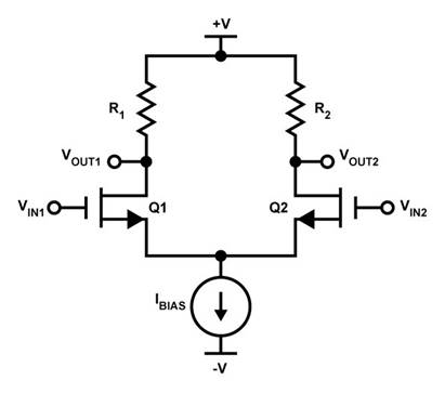
Note the following
v In real life, the current-source symbol would be replaced by a circuit that generates a constant current. (Refer to The Basic MOSFET Constant-Current Source for more information.) However, we want to keep things nice and simple for this introductory analysis, so in our simulations we’ll use an ideal current source instead of a constant-current circuit.
v An actual IC implementation of this circuit would replace the resistors with a current mirror functioning as an “active load.” However, if our goal is to understand the functionality of the differential pair, I think we should start with the resistor version.
v The differential pair is all about balance. Thus, for optimal performance the resistors and MOSFETs must be matched. This means that the channel dimensions of both FETs must be the same and that R1 must equal R2. The resistance value chosen for the two resistors will be referred to as RD (for drain resistance).
DC Analysis
Let’s determine the biasing conditions of this circuit when both inputs are grounded.
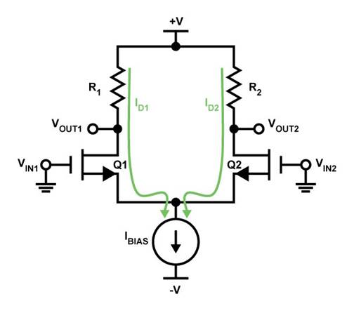
The sum of the two drain currents ID1 and ID2 must equal IBIAS. We also know that the two drain currents are equal because, in this idealized analysis, both halves of the circuit are identical. Thus,

Let’s assume for the moment that the transistors are in saturation. The equation for saturation-mode drain current is the following:

(We will ignore channel-length modulation throughout this article.) The drain current is already established (by the current source) and the gates are tied to the ground node; this means that the source voltage will settle on whatever value creates a gate-to-source voltage (VGS) corresponding to a drain current of IBIAS/2. We’ll let the simulation figure this out for us. The output voltages are easier: Calculate the voltage drop across the resistor as (IBIAS/2) × RD, then subtract this voltage drop from the positive supply. Here is an example:
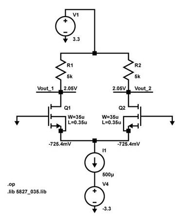
The output voltages are as expected. The source voltage seems reasonable considering that the threshold voltage (VTH) for this SPICE model is about 0.5 V; the simulation is telling us that the VGS corresponding to a drain current of 250 µA is about 0 V – (–725 mV) = 725 mV, which is about 225 mV above VTH.
Let’s go back to our assumption about the transistors being in saturation (aka “active mode”). A MOSFET amplifier needs to remain in the saturation portion of its transfer characteristic, because the gain is higher and more stable in the saturation region compared to the triode region. To ensure saturation, the drain voltage must always be higher than the gate voltage minus the threshold voltage:

In this example, the drain voltage (aka VOUT) is fixed at 2.05 V. This means that we have a restriction on VIN: the common-mode input voltage cannot exceed 2.05 V + 0.5 V = 2.55 V, because when the input voltage reaches VTH volts above the drain voltage, the MOSFET enters the triode region.
Common-Mode Rejection
Let’s do a quick simulation to prove to ourselves that the differential pair will not amplify common-mode voltages. Here is the circuit:
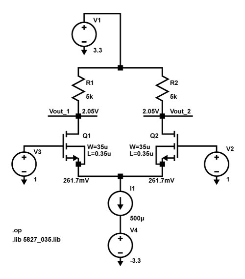
As you can see, even with a 1 V common-mode input, the output voltage is still at the bias voltage—2.05 V. A simple, conceptual explanation for this common-mode rejection behavior is the following: The magnitude of the output voltage is governed by the drain current, not the input voltage. As long as the two input voltages are the same, the fixed bias current is evenly divided between the two transistors, and thus VOUT1 and VOUT2 do not change.
Note also that the gate-to-source voltage is about the same (because the drain current hasn’t changed), though the source voltage has increased to compensate for the fact that the gate is now at 1 V instead of ground.
Differential Gain
You can understand this circuit’s differential action if you remember the following:

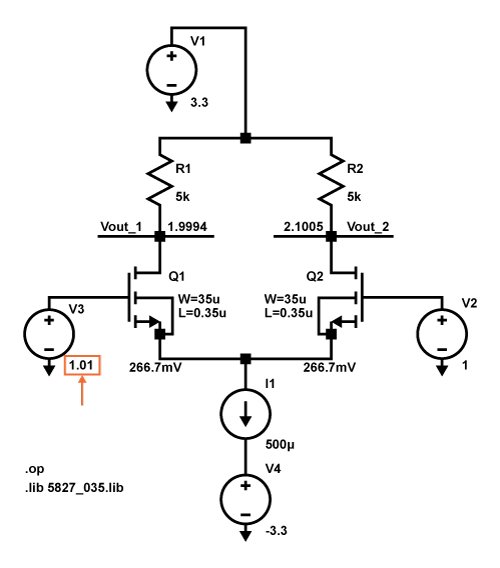
If the voltage at the gate of Q1 is higher than the voltage at the gate of Q2, VGS1 must also be higher than VGS2, because both transistors have the same potential at the source terminal. A higher gate-to-source voltage means more drain current, but the sum of the drain currents remains the same—thus, ID1 increases and ID2 decreases, and this causes a corresponding decrease in VOUT1 and a corresponding increase in VOUT2. For example:
We’ll finish up this introductory analysis by simulating the differential small-signal response and comparing the simulated gain to the theoretical gain. Let’s take the common-mode voltage back to 0 V and then apply a 1 mV sine wave to the gate of Q1:
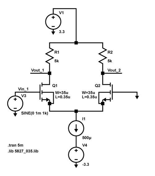
We will define the output voltage as VOUT1 – VOUT2; this doubles the gain relative to using only VOUT1 or VOUT2, and it also eliminates the DC offset associated with the bias voltages. Here is a plot with VIN1 and the differential output voltage:
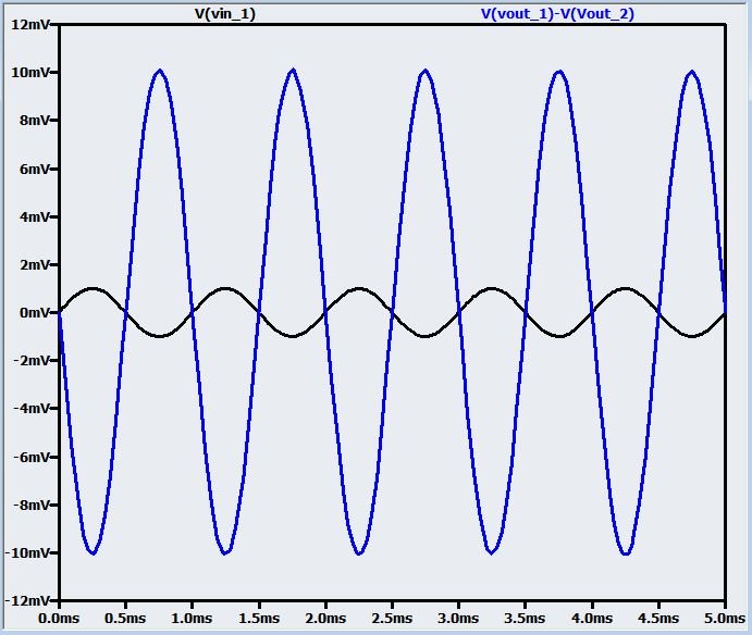
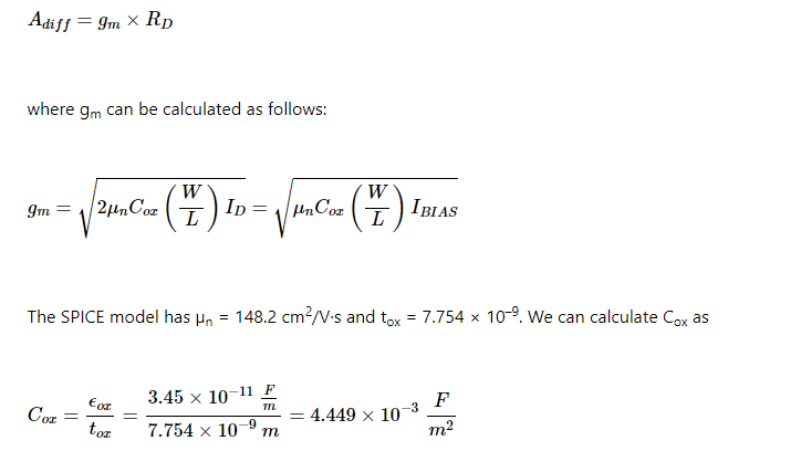
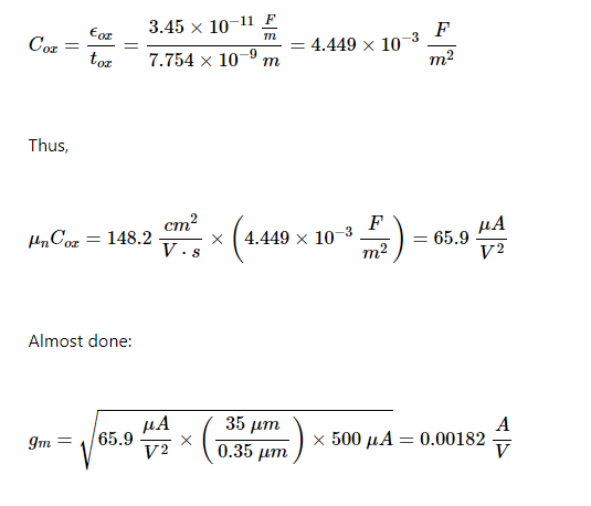
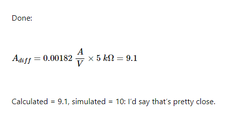
Here we have an output amplitude of 10 mV and an input amplitude of 1 mV; hence, our simulated differential gain is 10. The formula for theoretical differential gain is
Almost done:
Conclusion
The basic MOSFET differential pair is an important circuit for anyone who wants to delve into analog IC design. There is a lot more we could say about this circuit, but we’ll leave it here for now. In the next article, we’ll look at the improved performance that can be achieved by using an active load instead of drain resistors.