Darlington amplifier
The Darlington Transistor named after its inventor, Sidney Darlington is a special arrangement of two standard NPN or PNP bipolar junction transistors (BJT) connected together. The Emitter of one transistor is connected to the Base of the other to produce a more sensitive transistor with a much larger current gain being useful in applications where current amplification or switching is required.
Darlington Transistor pairs can be made from two individually connected bipolar transistors or a one single device commercially made in a single package with the standard: Base, Emitter and Collector connecting leads and are available in a wide variety of case styles and voltage (and current) ratings in both NPN and PNP versions.
As we saw in our Transistor as a Switch tutorial, as well as being used as an amplifier, the bipolar junction transistor, (BJT) can be made to operate as an ON-OFF switch as shown.
Bipolar Transistor as a Switch
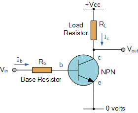
When the base terminal of the NPN transistor is grounded (0 volts), zero current flows into the base therfore Ib = 0. As the base terminal is grounded, no current flows from the collector to the emitter terminals therefore the non-conducting NPN transistor is switched “OFF” (cut-off). If we now forward biased the base terminal with respect to the emitter by using a voltage source greater than 0.7 volts, transistor action occurs causing in a much larger current to flow through the transistor between its collector and emitter terminals. The transistor is now said to be switched “ON” (conducting). If we operate the transistor between these two modes of cut-off and conduction, the transistor can be made to operate as an electronic switch.
However, the transistors base terminal needs to be switched between zero and some positive value much greater than 0.7 volts for the transistor to fully conduct. A higher voltage causes an increased base current, Ib to flows into the device resulting in collector current Ic becoming large while the voltage drop across the colletor and emitter terminals, Vce becomes smaller. Then we can see that a smaller current flowing into the base terminal can cause a much larger current to flow between the collector and the emitter.
The ratio of collector current to base current ( β ) is known as the current gain of the transistor. A typical value of β for a standard bipolar transistor may be in the range of 50 to 200 and varies even between transistors of the same part number. In some cases where the current gain of a single transistor is too low to directly drive a load, one way to increase the gain is to use a Darlington pair.
A Darlington Transistor configuration, also known as a “Darlington pair” or “super-alpha circuit”, consist of two NPN or PNP transistors connected together so that the emitter current of the first transistor TR1 becomes the base current of the second transistor TR2. Then transistor TR1 is connected as an emitter follower and TR2 as a common emitter amplifier as shown below.
Also note that in this Darlington pair configuration, the collector current of the slave or control transistor, TR1 is “in-phase” with that of the master switching transistor TR2.
Basic Darlington Transistor Configuration
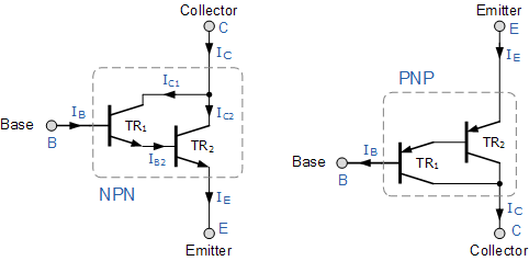
Using the NPN Darlington pair as the example, the collectors of two transistors are connected together, and the emitter of TR1 drives the base of TR2. This configuration achieves β multiplication because for a Base current ib, the collector current is β*ib where the current gain is greater than one, or unity and this is defined as:
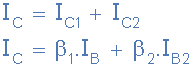
But the base current, IB2 is equal to transistor TR1 emitter current, IE1 as the emitter of TR1 is connected to the base of TR2. Therefore:
![]()
Then substituting in the first equation:
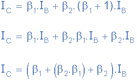
Where β1 and β2 are the gains of the individual transistors.
This means that the overall current gain, β is given by the gain of the first transistor multiplied by the gain of the second transistor as the current gains of the two transistors multiply. In other words, a pair of bipolar transistors combined together to make a single Darlington transistor pair can be regarded as a single transistor with a very high value of β and consequently a high input resistance.
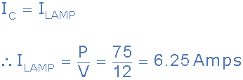
Darlington Transistor Example No1
Two NPN transistors are connected together in the form of a Darlington Pair to switch a 12V 75W halogen lamp. If the forward current gain of the first transistor is 25 and the forward current gain (Beta) of the second transistor is 80. Ignoring any voltage drops across the two transistors, calculate the maximum base current required to switch the lamp fully-ON.
Firstly, the current drawn by the lamp will be equal to the Collector current of the second transistor, then:
Using the equation above, the base current is given as:
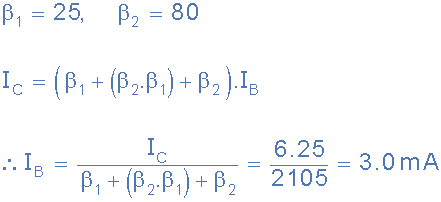
Then we can see that a very small base current of only 3.0mA, such as that supplied by a digital logic gate or the output port of a micro-controller, can be used to switch the 75 Watt lamp “ON” and “OFF”.
If two identical bipolar transistors are used to make a single Darlington device then β1 is equal to β2 and the overall current gain will be given as:
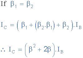
Generally the value of β2 is much greater than that of 2β, in which case it can be ignored to simplify the maths a little. Then the final equation for two identical transistors configured as a Darlington pair can be written as: