Hybrid - π equivalent circuits of BJTs
At low frequencies, we can analyze the transistor using h-parameters. But for high frequency, analysis of h-parameter model is not suitable for following reasons.
1. The values of h-parameters are not constant at high frequencies. So it is necessary to analyze transistor at each and every frequency which is impractical.
2. At high frequency h-parameters become complex in nature.
Due to the above reasons, modified T model and hybrid ∏ models are used for high frequency analysis of the transistor. These models give a reasonable compromise between accuracy and simplicity to do high frequency analysis of the transistor.
Hybrid - π common emitter transistor model
Common emitter circuit is most important practical configuration and this is useful for the analysis of transistor using hybrid - ∏ model. The following figure shows the hybrid - ∏ model for a transistor in CE configuration. For this model, all parameters are assumed to be independent of frequency. But they may vary with the quiescent operating point.
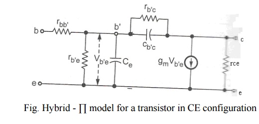
Elements in hybrid – π model
Cb’e and Cb’c :Forward biased PN junction exhibits a capacitive effect called diffusioncapacitance. This capacitive effect of normally forward biased base- emitter junction of the transistor is represented by Cb’e or Ce. The diffusion capacitance is connected between b’ and e represents the excess minority carrier storage in the base.
The reverse bias PN junction exhibits a capacitive effect called transition capacitance. This capacitive effect of normally reverse biased collector base junction of the transistor is represented by Cb’c or Cc.
rbb’:The internal node b’ is physically not accessible bulk node b represents external baseterminal.
rb’e: It is the portion of the base emitter which may be thought of as being in series withthe collector junction. This establishes a virtual base b’ for junction capacitances to be connected instead of b.
rb’c: Due to early effect, varying voltages across collector to emitter junction results inbase-width modulation. A change in the effective base -width causes the emitter current to change. This feedback effect between output and input is taken into account by connectinggb’c or rb’c between b’ and c.
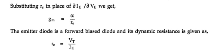
gm: Due to small changes in voltage Vb’eacross emitter junction, there is excess minoritycarrier concentration injected into the base which is proportional to Vb’e. So resulting small signal collector current with collector shorted to the emitter is also proportional to Vb’e.
gm is also called as transconductance and it is given as,

rce: It is the output resistance. It is also the result of early effect.
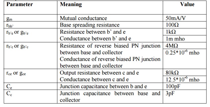
Hybrid – π parameter values
The following table shows the typical values for hybrid - π parameters at room temperature and for Ic = 1.3mA.
Hybrid – π conductances
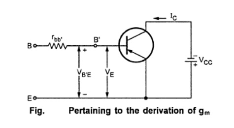
Transistor Transconductancegm
Let us consider a p-n-p transistor in CE configuration with Vcc bias in the collector circuit as shown in the above figure.
Transconductance gm is given as,
The collector current in active region is given as,
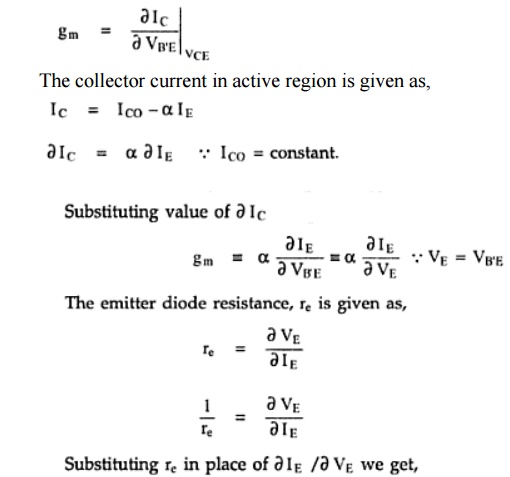
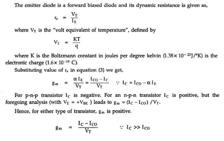
For Ic = 1.3mA, gm = 0.05mho or 50 mA/V. For Ic = 7.8mA, gm =
0.3mho or 300mA/V. These values are much larger than the transconductances
obtained with FETs.