MOSFET Amplifier
In our previous tutorial about FET amplifiers, we saw that simple single stage amplifiers can be made using junction field effect transistors, or JFET’s. But there are other types of field effect transistors available which can be used to construct and amplifier, and in this tutorial we will look at the MOSFET Amplifier.
Metal Oxide Semiconductor Field Effect Transistor, or MOSFET for short, is an excellent choice for small signal linear amplifiers as their input impedance is extremely high making them easy to bias. But for a mosfet to produce linear amplification, it has to operate in its saturation region, unlike the Bipolar Junction Transistor. But just like the BJT, it too needs to be biased around a centrally fixed Q-point.
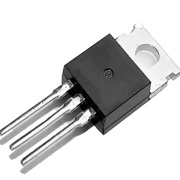
A Typical
MOSFET Transistor
MOSFETS conduct through a conductive region or path called “the channel”. We can make this conductive channel wider or smaller by applying a suitable gate potential. An electric field induced around the gate terminal by the application of this gate voltage affects the electrical characteristics of the channel, thus the name field-effect transistor.
In other words, we can control how the mosfet operates by creating or “enhancing” its conductive channel between the source and drain regions producing a type of mosfet commonly called an n-channel Enhancement-mode MOSFET, which simply means that unless we bias them positively on the gate (negatively for the p-channel), no channel current will flow.
There are large variations in the characteristics of different types of mosfets, and hence the biasing of a mosfet must be done individually. As with the bipolar transistor common emitter configuration, the common source mosfet amplifier needs to be biased at a suitable quiescent value. But first lets remind ourselves of the mosfets basic characteristics and configuration.
Enhancement N-channel MOSFET
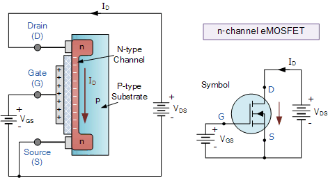
Note that the fundamental differences between a Bipolar Junction Transistor and a FET are that a BJT has terminals labelled Collector, Emitter and Base, while a MOSFET has terminals labelled Drain, Source and Gate respectively.
Also the MOSFET differs from the BJT in that there is no direct connection between the gate and channel, unlike the base-emitter junction of the BJT, as the metal gate electrode is electrically insulated from the conductive channel giving it the secondary name of Insulated Gate Field Effect Transistor, or IGFET.
We can see that for the n-channel MOSFET (NMOS) above the substrate semiconductor material is p-type, while the source and drain electrodes are n-type. The supply voltage will be positive. Biasing the gate terminal positive attracts electrons within the p-type semiconductor substrate under the gate region towards it.
This over abundance of free electrons within the p-type substrate causes a conductive channel to appear or grow as the electrical properties of the p-type region invert, effectively changing the p-type substrate into a n-type material allowing channel current to flow.
The reverse is also true for the p-channel MOSFET (PMOS), where a negative gate potential causes a build of holes under the gate region as they are attracted to the electrons on the outer side of the metal gate electrode. The result is that the n-type substrate creates a p-type conductive channel.
So for our n-type MOS transistor, the more positive potential we put on the gate the greater the build-up of electrons around the gate region and the wider the conductive channel becomes. This enhances the electron flow through the channel allowing more channel current to flow from drain to source leading to the name of Enhancement MOSFET.
Enhancement MOSFET Amplifier
Enhancement MOSFET, or eMOSFET, can be classed as normally-off (non-conducting) devices, that is they only conduct when a suitable gate-to-source positive voltage is applied, unlike Depletion type mosfets which are normally-on devices conducting when the gate voltage is zero.
However, due to the construction and physics of an enhancement type mosfet, there is a minimum gate-to-source voltage, called the threshold voltage VTH that must be applied to the gate before it starts to conduct allowing drain current to flow.
In other words, an enhancement mosfet does not conduct when the gate-source voltage, VGS is less than the threshold voltage, VTH but as the gates forward bias increases, the drain current, ID (also known as drain-source current IDS) will also increase, similar to a bipolar transistor, making the eMOSFET ideal for use in mosfet amplifier circuits.
The characteristics of the MOS conductive channel can be thought of as a variable resistor that is controlled by the gate. The amount of drain current that flows through this n-channel therefore depends on the gate-source voltage and one of the many measurements we can take using a mosfet is to plot a transfer characteristics graph to show the i-v relationship between the drain current and the gate voltage as shown.
N-channel eMOSFET I-V Characteristics
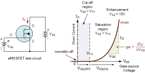
With a fixed VDS drain-source voltage connected across the eMOSFET we can plot the values of drain current, ID with varying values of VGS to obtain a graph of the mosfets forward DC characteristics. These characteristics give the transconductance, gm of the transistor.
This transconductance relates the output current to the input voltage representing the gain of the transistor. The slope of the transconductance curve at any point along it is therefore given as: gm = ID/VGS for a constant value of VDS.
So for example, assume a MOS transistor passes a drain current of 2mA when VGS = 3v and a drain current of 14mA when VGS = 7v. Then:
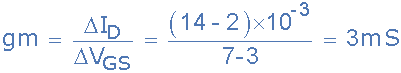
This ratio is called the transistors static or DC transconductance which is short for “transfer conductance” and is given the unit of Siemens (S), as its amps per volt. Voltage gain of a mosfet amplifier is directly proportional to the transconductance and to the value of the drain resistor.
At VGS = 0, no current flows through the MOS transistors channel because the field effect around the gate is insufficient to create or “open” the n-type channel. Then the transistor is in its cut-off region acting as an open switch. In other words, with zero gate voltage applied the n-channel eMOSFET is said to be normally-off and this “OFF” condition is represented by the broken channel line in the eMOSFET symbol (unlike the depletion types that have a continuous channel line).
As we now gradually increase the positive gate-source voltage VGS , the field effect begins to enhance the channel regions conductivity and there becomes a point where the channel starts to to conduct. This point is known as the threshold voltage VTH. As we increase VGS more positive, the conductive channel becomes wider (less resistance) with the amount of drain current, ID increases as a result. Remember that the gate never conducts any current as its electrical isolated from the channel giving a mosfet amplifier an extremely high input impedance.
Therefore the n-channel enhancement mosfet will be in its cut-off mode when the gate-source voltage, VGS is less than its threshold voltage level, VTH and its channel conducts or saturates when VGS is above this threshold level. When the eMOS transistor is operating in the saturation region the drain current, ID is given by:
eMOSFET Drain Current
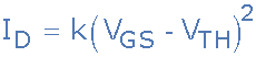
Note that the values of k (conduction parameter) and VTH (threshold voltage) vary from one eMOSFET to the next and can not be physically changed. This is because they are specific specification relating to the material and device geometry which are in-built during the fabrication of the transistor.
The static transfer characteristics curve on the right is generally parabolic (square law) in shape and then linear. The increase in drain current, ID for a given increase in gate-source voltage, VGS determines the slope or gradient of the curve for constant values of VDS.
Then we can see that turning an enhancement MOS transistor “ON” is a gradual process and in order for us to use the MOSFET as an amplifier we must bias its gate terminal at some point above its threshold level.
There are many different ways we can do this from using two separate voltage supplies, to drain feedback biasing, to zener diode biasing, etc, etc. But whichever biasing method we use, we must make sure that the gate voltage is more positive than the source by an amount greater than VTH. In this mosfet amplifier tutorial we will use the now familiar universal voltage divider biasing circuit.
DC Biasing the MOSFET
The universal voltage divider biasing circuit is a popular biasing technique used to establish a desired DC operating condition of bipolar transistor amplifiers as well as mosfet amplifiers. The advantage of the voltage divider biasing network is that the MOSFET, or indeed a bipolar transistor, can be biased from a single DC supply. But first we need to know where to bias the gate for our mosfet amplifier.
A mosfet device has three different regions of operation. These regions are called the: Ohmic/Triode region, Saturation/Linear region and Pinch-off point. For a mosfet to operate as a linear amplifier, we need to establish a well-defined quiescent operating point, or Q-point, so it must be biased to operate in its saturation region. The Q-point for the mosfet is represented by the DC values, ID and VGS that position the operating point centrally on the mosfets output characteristics curve.
As we have seen above, the saturation region begins when VGS is above the VTH threshold level. Therefore if we apply a small AC signal which is superimposed on to this DC bias at the gate input, then the MOSFET will act as a linear amplifier as shown.
eMOSFET DC Bias Point
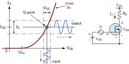
The common-source NMOS circuit above shows that the sinusoidal input voltage, Vi is in series with a DC source. This DC gate voltage will be set by the bias circuit. Then the total gate-source voltage will be the sum of VGS and Vi.
The DC characteristics and therefore Q-point (quiescent point) are all functions of gate voltage VGS, supply voltage VDD and load resistance RD.
The MOS transistor is biased within the saturation region to establish the desired drain current which will define the transistors Q-point. As the instantaneous value of VGS increases, the bias point moves up the curve as shown allowing a larger drain current to flow as VDS decreases.
Likewise, as the instantaneous value of VGS decreases (during the negative half of the input sine wave), the bias point moves down the curve and a smaller VGS results in a smaller drain current and increased VDS.
Then in order to establish a large output swing we must bias the transistor well above threshold level to ensure that the transistor stays in saturation over the full sinusoidal input cycle. However, there is a limit on the amount of gate bias and drain current we can use. To allow for maximum voltage swing of the output, the Q-point should be positioned approximately halfway between the supply voltage VDD and the threshold voltage VTH.
So for example, lets assume we want to construct a single stage NMOS common-source amplifier. The threshold voltage, VTH of the eMOSFET is 2.5 volts and the supply voltage, VDD is +15 volts. Then the DC bias point will be 15 – 2.5 = 12.5v or 6 volts to the nearest integer value.