JFET Bias Circuit
Junction Field Effect Transistor
In the Bipolar Junction Transistor tutorials, we saw that the output Collector current of the transistor is proportional to input current flowing into the Base terminal of the device, thereby making the bipolar transistor a “CURRENT” operated device (Beta model) as a smaller current can be used to switch a larger load current.
The Field Effect Transistor, or simply FET however, uses the voltage that is applied to their input terminal, called the Gate to control the current flowing through them resulting in the output current being proportional to the input voltage. As their operation relies on an electric field (hence the name field effect) generated by the input Gate voltage, this then makes the Field Effect Transistor a “VOLTAGE” operated device.

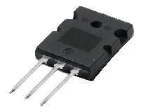
Typical Field Effect
Transistor
The Field Effect Transistor is a three terminal unipolar semiconductor device that has very similar characteristics to those of their Bipolar Transistor counterparts. For example, high efficiency, instant operation, robust and cheap and can be used in most electronic circuit applications to replace their equivalent bipolar junction transistors (BJT) cousins.
Field effect transistors can be made much smaller than an equivalent BJT transistor and along with their low power consumption and power dissipation makes them ideal for use in integrated circuits such as the CMOS range of digital logic chips.
We remember from the previous tutorials that there are two basic types of bipolar transistor construction, NPN and PNP, which basically describes the physical arrangement of the P-type and N-type semiconductor materials from which they are made. This is also true of FET’s as there are also two basic classifications of Field Effect Transistor, called the N-channel FET and the P-channel FET.
The field effect transistor is a three terminal device that is constructed with no PN-junctions within the main current carrying path between the Drain and the Source terminals. These terminals correspond in function to the Collector and the Emitter respectively of the bipolar transistor. The current path between these two terminals is called the “channel” which may be made of either a P-type or an N-type semiconductor material.
The control of current flowing in this channel is achieved by varying the voltage applied to the Gate. As their name implies, Bipolar Transistors are “Bipolar” devices because they operate with both types of charge carriers, Holes and Electrons. The Field Effect Transistor on the other hand is a “Unipolar” device that depends only on the conduction of electrons (N-channel) or holes (P-channel).
The Field Effect Transistor has one major advantage over its standard bipolar transistor cousins, in that their input impedance, ( Rin ) is very high, (thousands of Ohms), while the BJT is comparatively low. This very high input impedance makes them very sensitive to input voltage signals, but the price of this high sensitivity also means that they can be easily damaged by static electricity.
There are two main types of field effect transistor, the Junction Field Effect Transistor or JFET and the Insulated-gate Field Effect Transistor or IGFET), which is more commonly known as the standard Metal Oxide Semiconductor Field Effect Transistor or MOSFET for short.
The Junction Field Effect Transistor
We saw previously that a bipolar junction transistor is constructed using two PN-junctions in the main current carrying path between the Emitter and the Collector terminals. The Junction Field Effect Transistor (JUGFET or JFET) has no PN-junctions but instead has a narrow piece of high resistivity semiconductor material forming a “Channel” of either N-type or P-type silicon for the majority carriers to flow through with two ohmic electrical connections at either end commonly called the Drain and the Source respectively.
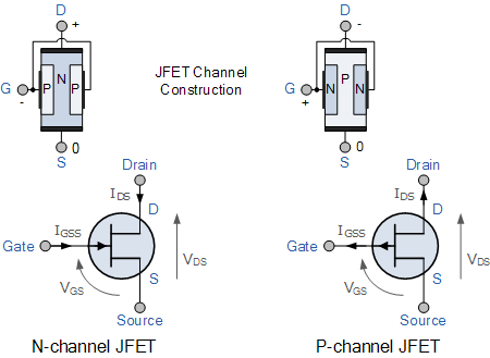
There are two basic configurations of junction field effect transistor, the N-channel JFET and the P-channel JFET. The N-channel JFET’s channel is doped with donor impurities meaning that the flow of current through the channel is negative (hence the term N-channel) in the form of electrons.
Likewise, the P-channel JFET’s channel is doped with acceptor impurities meaning that the flow of current through the channel is positive (hence the term P-channel) in the form of holes. N-channel JFET’s have a greater channel conductivity (lower resistance) than their equivalent P-channel types, since electrons have a higher mobility through a conductor compared to holes. This makes the N-channel JFET’s a more efficient conductor compared to their P-channel counterparts.
We have said previously that there are two ohmic electrical connections at either end of the channel called the Drain and the Source. But within this channel there is a third electrical connection which is called the Gate terminal and this can also be a P-type or N-type material forming a PN-junction with the main channel.
The relationship between the connections of a junction field effect transistor and a bipolar junction transistor are compared below.
Comparison of Connections between a JFET and a BJT
|
Bipolar Transistor (BJT) |
Field Effect Transistor (FET) |
|
Emitter – (E) >> Source – (S) |
|
|
Base – (B) >> Gate – (G) |
|
|
Collector – (C) >> Drain – (D) |
|
The symbols and basic construction for both configurations of JFETs are shown below.

The semiconductor “channel” of the Junction Field Effect Transistor is a resistive path through which a voltage VDS causes a current ID to flow and as such the junction field effect transistor can conduct current equally well in either direction. As the channel is resistive in nature, a voltage gradient is thus formed down the length of the channel with this voltage becoming less positive as we go from the Drain terminal to the Source terminal.
The result is that the PN-junction therefore has a high reverse bias at the Drain terminal and a lower reverse bias at the Source terminal. This bias causes a “depletion layer” to be formed within the channel and whose width increases with the bias.
The magnitude of the current flowing through the channel between the Drain and the Source terminals is controlled by a voltage applied to the Gate terminal, which is a reverse-biased. In an N-channel JFET this Gate voltage is negative while for a P-channel JFET the Gate voltage is positive.
The main difference between the JFET and a BJT device is that when the JFET junction is reverse-biased the Gate current is practically zero, whereas the Base current of the BJT is always some value greater than zero.
Biasing of an N-channel JFET

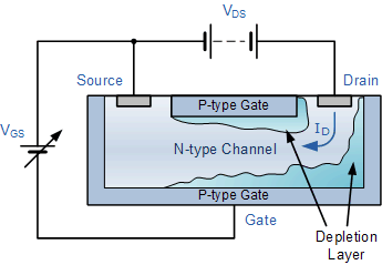
The cross sectional diagram above shows an N-type semiconductor channel with a P-type region called the Gate diffused into the N-type channel forming a reverse biased PN-junction and it is this junction which forms the depletion region around the Gate area when no external voltages are applied. JFETs are therefore known as depletion mode devices.
This depletion region produces a potential gradient which is of varying thickness around the PN-junction and restrict the current flow through the channel by reducing its effective width and thus increasing the overall resistance of the channel itself.
Then we can see that the most-depleted portion of the depletion region is in between the Gate and the Drain, while the least-depleted area is between the Gate and the Source. Then the JFET’s channel conducts with zero bias voltage applied (ie, the depletion region has near zero width).
With no external Gate voltage ( VG = 0 ), and a small voltage ( VDS ) applied between the Drain and the Source, maximum saturation current ( IDSS ) will flow through the channel from the Drain to the Source restricted only by the small depletion region around the junctions.
If a small negative voltage ( -VGS ) is now applied to the Gate the size of the depletion region begins to increase reducing the overall effective area of the channel and thus reducing the current flowing through it, a sort of “squeezing” effect takes place. So by applying a reverse bias voltage increases the width of the depletion region which in turn reduces the conduction of the channel.
Since the PN-junction is reverse biased, little current will flow into the gate connection. As the Gate voltage ( -VGS ) is made more negative, the width of the channel decreases until no more current flows between the Drain and the Source and the FET is said to be “pinched-off” (similar to the cut-off region for a BJT). The voltage at which the channel closes is called the “pinch-off voltage”, ( VP ).