DC Load Line for FET
The DC Load Line for FET circuit is drawn on the device output characteristics (or drain characteristics) in exactly the same way as for a BJT circuit. Refer to the n-channel FET circuit in Fig. 10-1. The source terminal is grounded, the gate is biased via resistor RG to a negative voltage (-VG), and the drain terminal is supplied from +VDD via resistor RD. The dc load line for this circuit is a graph of drain current (ID) versus drain-source voltage (VDS), for a given value of drain resistance and a given supply voltage.
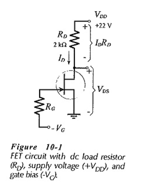
From Fig. 10-1, the drain-source voltage is,
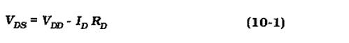
VDS = (supply voltage) – (voltage drop across RD)
Substituting VDD, RD, and convenient levels of ID into Eq. 10-1, produces corresponding VDS and ID values. These values are then plotted on the device characteristics, and the dc load line is drawn through them.
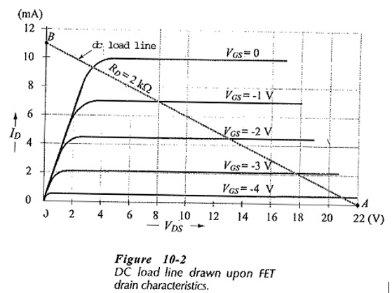
As already explained, the dc load line represents all corresponding ID and VDS levels that can exist in a FET circuit, as represented by Eq. 10-1. A point plotted at VDS = 16 V and ID = 10 mA on Fig. 10-2 does not appear on the load line, and so this combination of voltage and current cannot exist in this particular circuit (Fig. 10-1).
Bias Point (Q-Point)
Just as in the case of a BJT circuit, the dc bias point, or quiescent point (Q-point), identifies the device current and terminal voltages when there is no at input signal. When a signal is applied to the gate, ID varies according to the instantaneous amplitude of the signal, producing a variation in VDS.
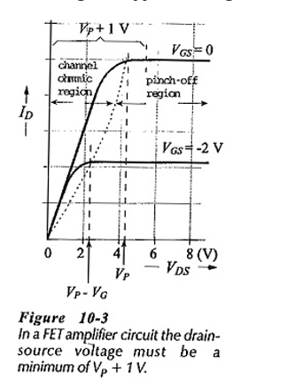
For a FET amplifier circuit, VDS must remain in the pinch-off region of the characteristics. This means that it must not be allowed to fall below the the device pinch-off voltage (Vp in Fig. 10-3), to avoid going into the channel ohmic region. Therefore, in a FET bias circuit the drain-source voltage should always be a minimum of (Vp + 1 V), as illustrated.
Where an external bias voltage (VG)
is included (as in Fig. 10-1), the pinch-off voltage for that bias level on the
device characteristics is (Vp – VG), (see Fig.
10-3). Consequently, the minimum drain-source voltage may be reduced to, 
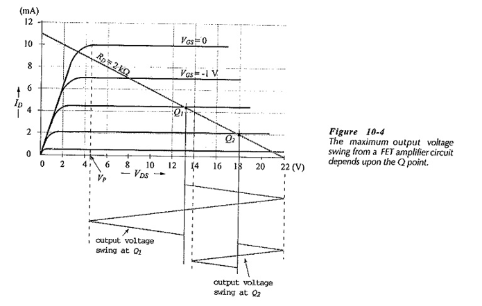
The bias point for a BJT can be selected half-way along the load line, to give the maximum possible symmetrical output voltage variation. To achieve the same result with a FET, the bias point must be half way between VDS = VDD and VDS = Vp. This is illustrated at Q1 in Fig. 10-4. When maximum VDS variations are not required, the FET bias point can be selected at any convenient point on the dc load line (Q2 in Fig. 10-4), just as in the case of a BJT amplifier.
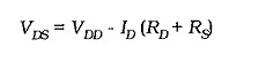
Effect of Source Resistor:
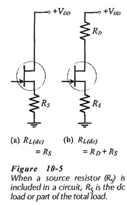
Figure 10-5(a) shows a circuit that has a resistor (RS) in series with the FET source terminal, and the supply voltage connected directly to the drain. In this case RS is the dc load, and Eq. 10-1 is rewritten as,
![]()
The dc load line is drawn exactly as discussed.
In Fig. 10-5(b) drain and source resistors RD and RS are both present, and the total dc load in series with the FET is (RD + RS). For drawing the dc load line, Eq. 10-1 is modified to,