Biasing BJT switching circuits
Activity: BJT device as a switch
Objective:
A bipolar junction transistor (BJT) can be used in many circuit configurations such as an amplifier, oscillator, filter, rectifier or just used as an on-off switch. If the transistor is biased into the linear region, it will operate as an amplifier or other linear circuit, if biased alternately in the saturation and cut-off regions, then it is being used as a switch, allowing current to flow or not to flow in other parts of the circuit. This lab activity describes the BJT when operated as a switch.
Background:
Switching circuits are significantly different than linear circuits. They are also easier to understand. Before investigating more complex circuits, we will begin by introducing discrete solid-state switching circuits: those built around BJTs.
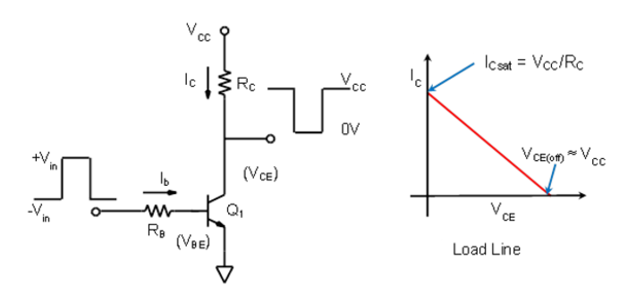
A switch consists of a BJT transistor that is alternately driven between the saturation and cutoff regions. A simple version of the switch is shown in figure 1. When the input equals -Vin , the base-emitter junction is reverse biased or off so no current flows in the collector. This is illustrated by the load line shown in the figure. When the BJT is in cutoff, the circuit (ideally) has the following values:
VCE = VCC and IC = 0 A
This state is similar to an open switch.
When the input equals +Vin, the transistor is driven into saturation and the following conditions occur:
VCE ˜ 0V and ICsat = VCC/RC
This state is similar to a closed switch connecting the bottom of RC to ground.

Figure 1 NPN BJT switch and its load line.
The characteristics for a BJT switch assume that:
1. -Vin is low enough to drive the transistor into cutoff.
2. +Vin must produce enough base current through RB to drive the transistor into saturation.
3. The transistor is an ideal component.
These conditions can be assured by designing the circuit so that:
1. -Vin = VBE
2. +Vin = VBE + IBRB (VCC is a good maximum)
3. IB > ICsat/ß
Condition 1 guarantees that the circuit is driven into the cutoff region by the input. Conditions 2 and 3 assure that the transistor will be driven into the saturation region.
An actual BJT switch differs from the ideal switch in several aspects. In practice, even in cutoff there is some leakage current through the transistor. Also, in saturation, there is always some voltage dropped across the transistor's internal resistance. Typically, this will be between 0.2 and 0.4 V in saturation depending on the collector current and size of the device. These variations from the ideal are generally minor with a properly sized device, so we can assume near ideal conditions when analyzing or designing a BJT switch circuit.
Materials:
Analog Discovery
Lab Instrument Hardware
Solder-less Breadboard
1 - 6.8KΩ Resistor (RB)
1 - 100Ω Resistor (RC)
1 - 5mm LED (any color)
1 - small signal NPN transistor (2N3904)
Directions:
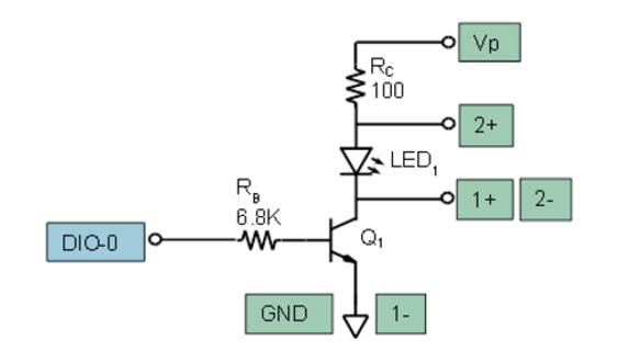
One common application for a BJT (or any other) switch is to drive an LED. An LED driver is shown in figure 2. The driver shown in this figure is used to couple a low current part of the circuit to a relatively high current device (the LED). When the output from the low current circuit is low (0 V), the transistor is in cutoff and the LED is off. When the output from the low current circuit goes high (+3.3 V), the transistor is driven into saturation and the LED lights. The driver is used because the low-current part of the circuit may not have the current capability to supply the 20 mA (typical) required to light the LED to full brightness.
Build the LED switch circuit shown in figure 2 on your solder-less breadboard. RC serves to limit the current that flows in the LED from the +5 V power supply (Vp). The switch is controlled by digital output DO from the Discovery connector. Scope channel 1 will display the voltage across the switch transistor Q1 (VCE) and scope channel 2 will display the voltage across the LED.

Figure 2, NPN LED switch