Differential amplifiers
The differential amplifier is probably the most widely used circuit building block in analog integrated circuits, principally op amps. We had a brief glimpse at one back in Chapter 3 section 3.4.3 when we were discussing input bias current. The differential amplifier can be implemented with BJTs or MOSFETs. A differential amplifier multiplies the voltage difference between two inputs (Vin+ - Vin-) by some constant factor Ad, the differential gain. It may have either one output or a pair of outputs where the signal of interest is the voltage difference between the two outputs. A differential amplifier also tends to reject the part of the input signals that are common to both inputs (Vin+ + Vin-)/2 . This is referred to as the common mode signal.
Starting with the basics
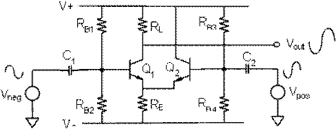
It is often easiest to start again with the very basic single transistor and build a workable differential amplifier as a logical progression from there. Consider the single transistor amplifier stage, figure 12.1.1, which is similar to what we explored in the section on the degenerated common emitter back in Chapter 9. This amplifier can actually be viewed as either an inverting common emitter amplifier when driven from Vneg and with Vpos considered an AC ground. Or as a non-inverting common base amplifier when driven from Vpos and with Vnegconsidered an AC ground.
Figure 12.1.1 AC coupled difference amplifier
Let's assume that we make the coupling capacitors, C1 and C2, sufficiently large so that we can view them as AC shorts for the signal frequencies of interest. The small signal voltage gain from Vneg to Vout is:
![]()
Likewise, the small signal voltage gain from Vpos to Vout is:
![]()
The transistor amplifies the small signal voltage across its Vbe which in this case is Vpos-Vneg. If we apply equal amplitude, in phase signals to Vposand Vneg, such that Vpos-Vneg = 0 then there will be no varying signal across Vbe and the output signal at Vout will be zero. On the other hand, if we apply equal amplitude signals that are 180º out of phase with each other, then Vpos-Vneg = twice the amplitude of the inputs. This difference voltage will appear across Vbe and be amplified by gm*RL at Vout.
The inverting or negative input terminal of our simple difference amplifier has the relatively high input impedance of the common emitter stage while the non-inverting or positive input terminal of the amplifier has the relatively low input impedance of the common base stage. The importance of this observation and how it can be put to good use will become apparent in the next chapter (13) on transimpedance amplifiers. It would be advantageous if our differential amplifier had more symmetric inputs where the input impedance for both the positive and negative inputs was as high as possible, ideally infinite. An additional step to get us in that direction is shown in figure 12.1.2. If we now include an emitter follower stage, Q2, to buffer the relatively low impedance of the common base amplifier path of the positive input we get a more symmetrical pair of inputs.
Figure 12.1.2 difference amplifier with emitter follower added.
Because we are still AC coupling our input signals a second set of biasing resistors, RB3 and RB4 are necessary to provide DC bias for the new emitter follower. If we instead DC couple the now symmetric inputs the biasing resistors become unnecessary and our difference amplifier now takes on the look of the classic differential pair we will discuss in the next section.
Long-tailed pair
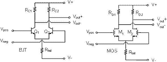
Figure 12.2.1: A long-tailed pair with resistor loads
The classic differential pair amplifier is formed from at least two identical transistors, configured with the emitters for BJT transistors or the sources for FETs connected together. A long-tailed pair (LTP), or emitter coupled (source coupled) pair, is a pair of transistors where the shared emitter or source node is supplied from a more or less constant current source/sink, which could be as simple as a relatively large value resistor connected to the negative supply, such as Rtail in figure 12.2.1, (or the positive supply for p-type devices) that develops a large voltage drop relative to the amplitude of the input signal thus the “long tail”. Given the more or less constant current supplied to the emitters or sources the summation of the two collector or drain currents is also more or less constant with signal.
The two inputs at the bases or gates can be fed with a differential or balanced input signal and the two outputs from the collectors or drains remain balanced, or one input could be grounded to convert a single ended input signal to a differential output. The higher the resistance of the current source Rtail, the lower the common mode gain or Ac is, and the better the common mode rejection ratio (CMRR). In more sophisticated designs, an active constant current source may be substituted for the high resistance Rtail. With two inputs and two outputs, this forms a differential amplifier stage. The two bases or gates are inputs which are differentially amplified by the pair.
Even though this circuit is designed to have two inputs and two outputs, it is not necessary to use both inputs and both outputs. (Remember, a differential amplifier was defined as having two possible inputs and two possible outputs.) A differential amplifier can be connected as a single-input, single-output device; a single-input, differential-output device; or a differential-input, differential-output device. The output may be single-ended (taken from just one of the collectors or drains, or differential depending on the needs of the subsequent circuitry.
In a long-tailed pair built using BJTs, the emitters are connected together, and then through the current source to ground or to a negative supply (for an LTP using NPN transistors). In this form, one of the transistors can be thought of as an amplifier operating in common emitter configuration, and the other as an emitter follower, feeding the other input signal into the emitter of the first stage as we discussed in the previous section. Since a transistor will amplify the current flowing between base and emitter, it follows that the current flowing in the collector circuit of the first transistor is proportional to the difference between the two inputs. However since the circuit is totally symmetrical, either element can be viewed as an amplifier or as a follower, understanding how the circuit functions does not depend on which role you assign to which device.
The bias condition assumes equal voltages at Vpos and Vneg, forcing the bias current Itail (set by Rtail) to split equally between the transistors resulting in IC1 = IC2. With RC1 = RC2, equal voltages develop at Vout+ and Vout-. Using MOSFETs, we can construct an source-coupled differential pair, which is a counterpart of the emitter-coupled differential pair using BJTs. The main advantage of using MOSFETs for a differential pair compared to BJTs is the nearly infinite input impedance, while the disadvantage is generally lower differential gain.
Assuming the two MOSFETs are the same. The analysis of the source-coupled differential pair proceeds in the same way as the emitter-coupled differential pair for both common-mode signal and differential input signal. The transfer characteristics for drain current Id1 and Id2 are shown in the figure.
Differential Gain
We can calculate the differential voltage gain as follows. Consider Q1 and Q2 as current sources controlled by their base voltages. RC1 and RC2 then convert the currents back into voltages. First, the small signal collector current
![]()
Where the transconductance gm (Amps/Volts) is set by the DC collector current
 at room
temperature.
Then, RC converts Ic back to a voltage.
![]()
Bringing the input Vdiff = Vpos - Vneginto the picture, notice it divides equally across the two base-emitter junctions, but with opposite polarities. Putting it all together you get a single-ended output at each collector


Subtracting the two outputs gets you a differential output of
![]()
An example to set the bias: Rtail sets the bias at Ie = (-0.6V - VDD) / Rtail = (-0.6 V - (-15 V)) / 7.2 kΩ = 2 mA which divides equally between Q1 and Q2giving
![]()
Finally, we easily calculate gm = 1 mA / 25 mV = 0.04 A/V. The single-ended gain becomes:

The output from a differential amplifier is itself often differential. If this is not desired, then only one output can be used, disregarding the other output. Or to avoid sacrificing gain, a differential to single-ended stage can be used following the differential stage. This is often implemented with an active current mirror load instead of the collector/drain resistors.
Long-tailed pairs are frequently used in circuits that implement linear amplifiers with feedback, as in operational amplifiers, and in other circuits that require a differential amplifier.
When used as a switch, the “left” base or gate is used as signal input and the “right” base or gate is grounded; output is taken from the right collector or drain. When the input is zero or negative, the output is close to zero; when the input is positive, the output is most-positive, dynamic operation being the same as the amplifier use described above.
Bias stability and independence from variations in device parameters can be improved by negative feedback introduced via emitter or source degeneration resistors.
The differential pair with a small differential input signal vi
Small-Signal Operation
![]()
Some Formulas
1. Differential Input Resistance
![]()
2. Differential Voltage gain

3. Common mode gain:


Increasing the linear differential input range of the diff pair
Sometimes it is advantageous to add emitter degeneration resistor REF to the circuit, as shown in the figure 12.3.1. The resistors have the disadvantage of reducing the differential voltage gain of the circuit. However, two reasons for this is to increase input impedance and to reduce distortion due to the nonlinearity of the BJTs. The right figure shows the transfer characteristic of the differential amplifier (REF=40VT/IEE).
To improve linearity, we introduce emitter-degeneration resistors, which increase the linear range from a few VT to about ITailR.
The current mirror as a load
The following figure shows a variation of the emitter-coupled pair in which the collector resistors are replaced by a current mirror. This circuit is particularly favored in integrated circuits, because matched transistors are much easier to construct than precession matched high value resistors. A simple analysis by assuming large ß so that base currents of Q3 and Q4 are neglected, results in the equation as follows:

For
![]()
is approximately proportional to vid. Notice furthermore that the common-mode input component does not affect the output current.


