Methods of Transistor Biasing
The biasing in transistor circuits is done by using two DC sources VBB and VCC. It is economical to minimize the DC source to one supply instead of two which also makes the circuit simple.
The commonly used methods of transistor biasing are
- Base Resistor method
- Collector to Base bias
- Biasing with Collector feedback resistor
- Voltage-divider bias
All of these methods have the same basic principle of obtaining the required value of IB and IC from VCC in the zero signal conditions.
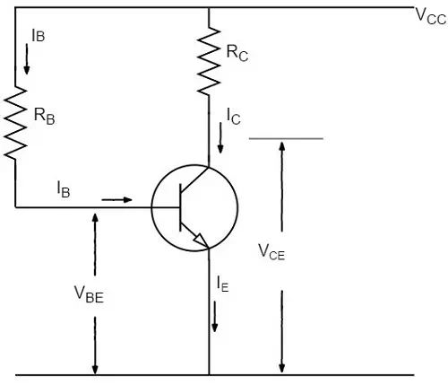
Base Resistor Method
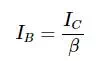
In this method, a resistor RB of high resistance is connected in base, as the name implies. The required zero signal base current is provided by VCC which flows through RB. The base emitter junction is forward biased, as base is positive with respect to emitter.
The required value of zero signal base current and hence the collector current (as IC = βIB) can be made to flow by selecting the proper value of base resistor RB. Hence the value of RB is to be known. The figure below shows how a base resistor method of biasing circuit looks like.
Let IC be the required zero signal collector current. Therefore,
This circuit helps in improving the stability considerably. If the value of ICincreases, the voltage across RL increases and hence the VCE also increases. This in turn reduces the base current IB. This action somewhat compensates the original increase.
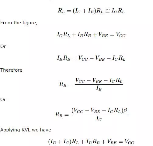
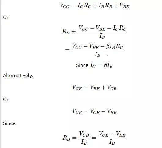
The required value of RB needed to give the zero signal collector current ICcan be calculated as follows.
The required value of RB needed to give the zero signal current IC can be determined as follows.
Suppose that the current flowing through resistance R1 is I1. As base current IB is very small, therefore, it can be assumed with reasonable accuracy that current flowing through R2 is also I1.
Now let us try to derive the expressions for collector current and collector voltage.
Collector Current, IC
From the circuit, it is evident that,
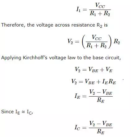
From the above expression, it is evident that IC doesn’t depend upon β. VBE is very small that IC doesn’t get affected by VBE at all. Thus IC in this circuit is almost independent of transistor parameters and hence good stabilization is achieved.
Collector-Emitter Voltage, VCE
Applying Kirchhoff’s voltage law to the collector side,
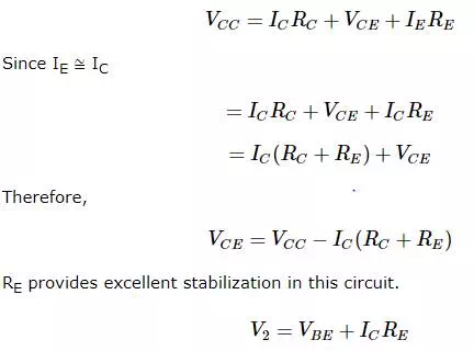
Suppose there is a rise in temperature, then the collector current ICdecreases, which causes the voltage drop across RE to increase. As the voltage drop across R2 is V2, which is independent of IC, the value of VBEdecreases. The reduced value of IB tends to restore IC to the original value.
Stability Factor
The equation for Stability factor of this circuit is obtained as
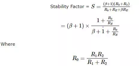
If the ratio R0/RE is very small, then R0/RE can be neglected as compared to 1 and the stability factor becomes
![]()
This is the smallest possible value of S and leads to the maximum possible thermal stability.