JFET Operation-pinchoff voltage-drain current
Operation of JFET
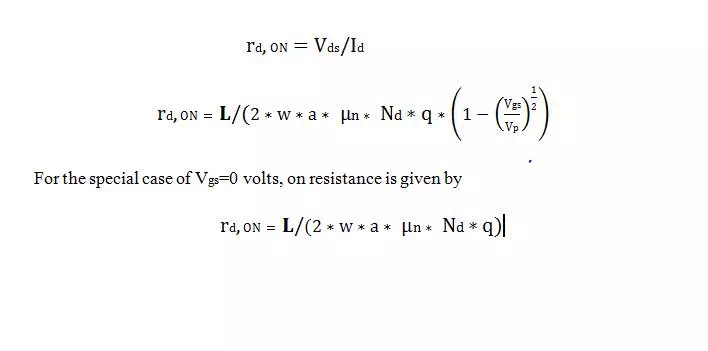
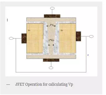
Consider an N-channel JFET, analogous to base current in Bipolar Junction transistor gate voltage is used to control the current through the channel. With gate to source voltage at zero volts, application of even small positive drain to source voltage causes drain current to flow from drain to source through channel.
As we reverse bias gate to by applying negative voltage to P-type gate, the depletion layer width’s on either side of the channel increases. So increasing the reverse bias of gate terminal decreases the effective width of the channel. Hence the drain current will be less than the value of it when no reverse bias is applied to gate. For small applied Vds the channel is nearly uniform, JFET simply acts as a voltage controlled resistance. The gate to source voltage dictates the resistance offered by channel to drain current. This is due to the fact that as -Vgs is increased i.e increasing the reverse bias the depletion layer width increases. So conductivity of channel decreases, hence it offers more resistance to current flow.
Pinch off Voltage
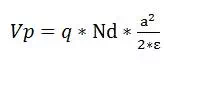
As we continue to increase the reverse bias of gate terminal the depletion layer widens and a point is reached where entire channel is filled with depletion layer and drain current will be reduced to zero except for small reverse saturation currents order of nano amperes. The gate to source voltage at which at which the entire channel will be depleted of charge carrier is called pinch-off voltage.
Where Vgs is Gate to source voltage
Vp is pinch off voltage
Vgd is gate to drain voltage
Where Vds is Drain to source voltage
Assume the two junctions between the p-type semiconductors and N-type channel are abrupt and Na >> Nd so that Wn >> Wp+, the space charge width (this can be obtained by solving Poisson’s equation for abrupt junction) is given by
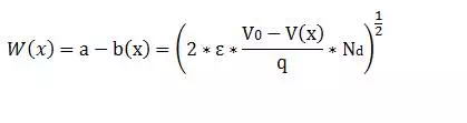
Where
Nd is donor impurity concentration,
ε is the dielectric strength of the channel
V(x) is the applied potential at distance x from source end.
When Vgs= Vp Then channel completely gets blocked and drain current is zero b(x)=0 and V(x) =0 we obtain
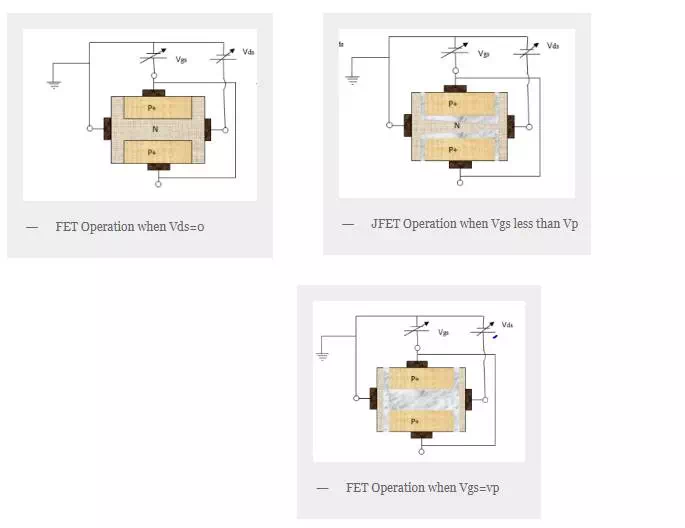
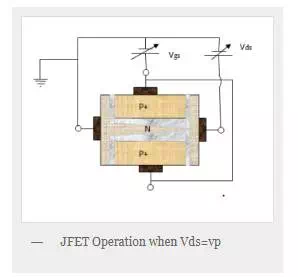
Similarly keeping Vgs fixed increase Vds continuously. The channel will be depleted more at the drain end of the channel due to the fact positive drain voltage reverse biases the p+-n junction and this drain to source voltage fall gradually from the value of Vdd to zero at source end. When the reverse bias at drain end Vgd falls below Vp the channel will get pinched off at drain end and drain current saturates.
FET
Drain Current at small at small drain to source voltage
The FET drain current at flowing through the channel will be entirely drift current, so the equation for drain current is given by
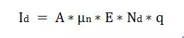
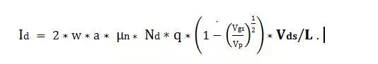
Where A is the area of the surface normal to current flow=2*W*b(x), W is the width of semi conductor bar, is mobility of electrons, E is the electric field applied, Nd is donor concentration. This equation is written based on the assumption that the intrinsic concentration of electrons in N-channel is less and conduction band electronic charge density Ne- = Nd. Substituting the value of b(x) from the equation given for W(x) in equation for drain current and rearranging the terms we get
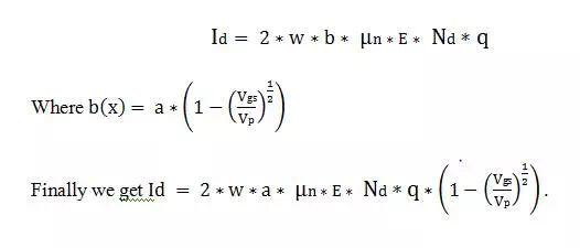
For small values of Vds the electric field produced by Vds can be assumed to be uniform and if this holds we can substitute E = Vds/L where L is the length of semi conductor bar. Therefore
On resistance: The on resistance of JFET can be obtained from the equation for Id by defining it as