High frequency hybrid Pi or Giacoletto model of BJT
Introduction
The low frequency small signal model of bipolar junction transistor crudely holds for frequencies below 1 MHz. For frequencies greater than 1 MHz the response of the transistor will be limited by internal and parasitic capacitance’s of the bipolar junction transistor. Hence at high frequencies the low frequency small signal model of transistorhas to be modified to include the effects of internal and parasitic capacitance’s of bipolar junction transistor. These capacitance’s limit the usage of BJT at higher frequencies.Thus in order to estimate the gain and switching on and off times of BJT at higher frequencies the high frequency model of BJT has to be used to get reasonably accurate estimates.The high frequency hybrid pi model is also called as Giacoletto model named after L.J.Giacoletto who introduced it in 1969.
High frequency effects on BJT
§ The gain decreases at high frequencies due to internal feedback capacitance’s.The highest frequency of operation of BJT will be limited by internal capacitance’s of BJT.
§ The on and off switching times of BJT will be high and speed will be limited due to internal charge storage effects.
High frequency model of BJT
The high frequency parameters of BJT may vary with operating point but the variation is negligible for small signal variations around the operating point. Following is the high frequency model of a transistor.
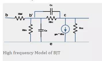
Where
B’ = internal node in base
Rbb’ = Base spreading resistance
Rb’e = Internal base node to emitter resistance
Rce = collector to emitter resistance
Ce = Diffusion capacitance of emitter base junction
Rb’c = Feedback resistance from internal base node to collector node
gm = Transconductance
CC= transition or space charge capacitance of base collector junction.
Physical explanation of parameters of high frequency model of BJT
Rbb’ is the base spreading resistance of BJT which represents the bulk resistance of the material between the base terminal and the physical inaccessible internal node of BJT. Typically it is of the order of 100’s of ohms.
Rb’e is the Internal base node to emitter resistance. It accounts for the increase recombination base current as emitter current increases. It is in parallel with the collector circuit and hence reduces the collector current value from emitter current.This resistance will be high order of kilo ohms as the decrease in the collector current due to base recombination currents will be very less.
Rb’c is the Feedback resistance from internal base node to collector node. It is included in the model to take in to account early effect.As collector to base reverse bias is increased(action) the effective width increases and collector current increases(feedback response).This feedback effect(early effect) is accounted for by Rb’c.
Rce represents the bulk resistance of the material between collector to emitter.
Ce is the Diffusion capacitance of emitter base junction. Diffusion capacitance of emitter base junction is directly proportional to emitter bias current and forward base transit time. Forward transit time is defined as the average time the minority carrier spends in base. The Diffusion capacitance of emitter base junction accounts for the minority charge stored in base and is given as
Ce = τF*IE/VT
where IE is emitter bias current
VT is voltage equivalent of temperature = k*T/e =26 mV at 27 Deg C
τF is forward base transit time given as τF = W2/(2*DB)
W is effective base width
DB is diffusion constant for minority carriers in base holes in PNP transistor and electrons in NPN transistor.
Ce is a function of temperature as DB = VT*μ (μ varies as T-m) is a function of temperature. Ce can be found theoretically from unit gain frequency and Transconductance as follows
Ce = gm/(2*pi*fT)
Unity gain
frequency is defined as frequency at which the current gain of transistor
reduces to unity. The 3 db higher cutoff frequency of BJT is termed as beta
frequency of BJT denoted by fβ. The beta frequency
and Unity gain frequency are related as
fT = hfe*fβ
where hfe is current gain of BJT in CE configuration.
CC represents the transition or space charge capacitance of base collector junction.The transition capacitance of base collector junction is given as
Cj = Co/(1+VCB/VBV)n
where Co is the transition capacitance for zero collector to base bias
VCB is collector to base bias
VBV is the built in voltage across base collector junction
n is a constant called as grading coefficient varies form o.25 to 0.5.
The high frequency hybrid Pi or Giacoletto model of BJT is valid for frequencies less than the unit gain frequency.
High frequency model parameters of a BJT in terms of low frequency hybrid parameters
The main advantage of high frequency model is that this model can be simplified to obtain low frequency model of BJT. This is done by eliminating capacitance’s from the high frequency model so that the BJT responds without any significant delay(instantaneously) to the input signal. In practice there will be some delay between the input signal and output signal of BJT which will be very small compared to signal period(1/frequency of input signal) and hence can be neglected. The high frequency model of BJT is simplified at low frequencies and redrawn as shown in the figure below along with the small signal low frequency hybrid model of BJT
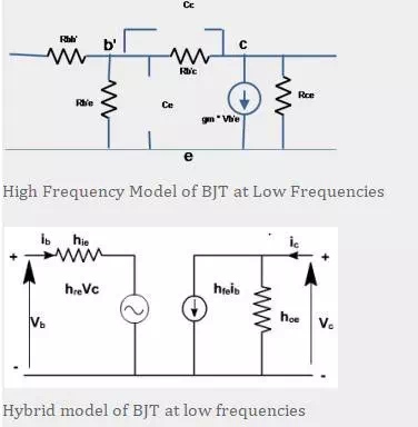
The High frequency model parameters of a BJT in terms of low frequency hybrid parameters is given below
Transconductance gm = Ic/Vt
Internal Base node to emitter resistance rb’e = hfe/ gm = (hfe* Vt )/ Ic
Internal Base node to collector resistance rb’e = (hre* rb’c) / (1- hre) assuming hre << 1 it reduces to rb’e = (hre* rb’c)
Base spreading resistance rbb’ = hie – rb’e = hie – (hfe* Vt )/ Ic
Collector to emitter resistance rce = 1 / ( hoe – (1+ hfe)/rb’c)